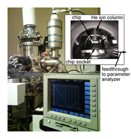
Graphene’s potential for nanoelectronics applications is limited by the shortcomings of current techniques for its fabrication, typically electron beam lithography with reactive ion etching or chemical processes, which can return irregularly shaped graphene flakes or disordered edges.
David C. Bell, Max C. Lemme, and colleagues at Harvard and MIT report the use of a Helium Ion Beam microscope configured for lithography to etch graphene devices with sub-20nm feature sizes. As a direct-write process, helium ion lithography bypasses the need for resists or other materials to come in contact with the graphene, allowing the devices to be fabricated cleanly and without damage.
Further, the authors present in situ electrical measurement during lithography and controllably modify the electrical properties of the devices.
This work was reported in arXiv.
arXiv:0905.4409v1 Etching of Graphene Devices with a Helium Ion Beam (submitted May 27, 2009)
arXiv:0905.4407v1 Precision Cutting and Patterning of Graphene with Helium Ions (submitted May 27, 2009)
Nanotechweb.org Technology Update
Image credit: Harvard University
