
| Electrochemical deposition techniques offer an alternative method for grafting nanostructured materials on a graphene surface. Kim et. al. report an innovative approach to directly integrate CdSe quantum confined nanostructures with graphene basal planes. |
Reviewed by Jeff Morse, PhD., National Nanomanufacturing Network
Graphene has received significant attention in recent years as a promising material for a range of applications due to its unique electrical, mechanical, and chemical properties. With recent demonstrations of large-scale production of high quality films, graphene is being investigated for potential use as transparent electrodes for solar cells, sensors, and nanoelectronics due to extremely high electron mobility. In order to exploit the full potential of this emerging material in these and other application areas, surface grafting or integration of functional materials and structures on graphene would be an invaluable method once fully developed.
Surface grafting techniques face challenges due the lack of reactivity of the graphene basal plane, which exhibits a lower chemical potential than the edges or defect sites. This problem may be addressed via vacuum techniques to modify the graphene surface, such as ozone treatment, forming a metal underlayer, or grafting of organic molecules having specific functional groups, although these techniques do not alter the surface potential difference between the basal plane and the defects/edge.
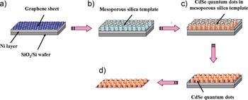
Subsequent atomic force microscopy (AFM) imaging of the deposited CdSe nanostructures shows a densely packed array having height ranging from 5-12nm, with 10nm diameter, and 14nm between each structure. Compared with CdSe films electrochemically deposited on graphene surfaces without the mesoporous silica template, the templated nanostructures were in fact close packed in a uniform hexagonal array; the unpatterned graphene surface exhibited CdSe deposits forming lines in closed loop configurations, most likely replicating the edges of the individual graphene sheets. The AFM imaging also demonstrated enhanced density for the electrochemically deposited nanostructure, which is likely a result of the underlying Ni layer below the graphene film. The Ni layer provided uniform potential distribution during the electrochemical deposition step, suggesting that the nanochannels formed by the silica template exert resistance against electrolyte diffusion during the deposition process, thereby equalizing the potential distribution in order to suppress preferential deposition at the edge or defect sites.
Kim et. al. report an innovative approach to directly integrate CdSe quantum confined nanostructures with graphene surfaces. Their work may impact the enhancement of electrical, mechanical, and physical properties for graphene-based materials and devices for implementation in a range of future applications.
Image reproduced from KimYT, et. al. 2009. Electrochemical Synthesis of CdSe Quantum Dot Arrays on a Graphene Basal Plane Using Mesoporous Silica Thin-Film Templates. Advanced Materials 21: 1–4. DOI: 10.1002/adma.200902736. Copyright Wiley-VCH Verlag GmbH & Co. KGaA. Reproduced with permission.
.