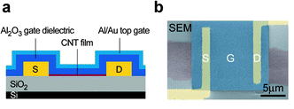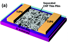
Recent efforts to synthesize carbon nanotube networks in a transistor integration strategy have shown significant promise as an alternative technology for large area TFT applications. With new knowledge of necessary process control mechanisms and carbon nanotube network properties, these approaches use solution-based assembly techniques to achieve specific device parameters by design and have the potential to gain a foothold in a high-end consumer products markets.
Single walled carbon nanotubes (SWCNT) have gained significant attention over the past decade due to potentially superior electronic, mechanical, and chemical properties. For nanoelectronic applications, transistors fabricated from individual SWCNTs exhibit very high carrier mobility, yet have limited current carrying ability due to their nanoscale size. Furthermore, practical approaches to fabricate large scale integrated circuits have not yet been realized. In contrast, TFT applications simply require sufficient device characteristics (On/Off ratio, on-state conductance, and carrier mobility) in a thin, nominally transparent design configuration and can be fabricated by low-cost, scalable processes. Progress in device synthesis has been limited by the chirality properties of the SWCNT networks, which typically contain a mixture of semiconducting and metallic CNTs. As the SWCNTs are assembled in an overlapping configuration between the source and drain of the transistor, percolation transport through metallic nanotubes limits the device on/off ratio, yet enables high current handling capability. Rigorous purification processes have been used to yield SWCNT networks composed primarily of semiconducting nanotubes.
A handful of studies published within the last year have focused on the process of integrating SWCNT networks into TFTs with very positive outcomes for industrial scale up. The knowledge gained from this nanomanufacturing research has provided sufficient progress suggesting these approaches may be suitable for rigorous process scale-up for specific applications. With key metrics for TFT devices being demonstrated, applications realizing an immediate benefit from this manufacturing approach include displays, lighting, and electronic paper. This month we take a closer look at three key papers in this area that have fostered significant interest within the community.


It should be acknowledged that the findings of each of the investigations cited abovehave provided critical insights into the physics and phenomenon of current transport in mixed chirality CNT networks providing the basis for developing transistor design strategies conducive to large area TFT applications. With this emphasis, the nanomanufacturing community will look forward to future commercialization of this technology.
References
- Engel M, Small JP, Steiner M, Freitag M, Green AA, Hersam MC, and Avouris P. 2008. Thin Film Nanotube Transistors Based on Self-Assembled, Aligned, Semiconducting Carbon Nanotube Arrays. ACS Nano 2 (12): 2445–2452. DOI: 10.1021/nn800708w.
- LeMieux MC, Sok S, Roberts ME, Opatkiewicz JP, Liu D, Barman SN, Patil N, Mitra S, and Bao Z. Solution Assembly of Organized Carbon Nanotube Networks for Thin-Film Transistors. ACS Nano, Article ASAP 19 November 2009. DOI: 10.1021/nn900827v.
- Wang C, Zhang J, Ryu K, Badmaev A, Gomez De Arco L, and Zhou C. 2009. Wafer-Scale Fabrication of Separated Carbon Nanotube Thin-Film Transistors for Display Applications. Nano Letters 9 (12): 4285–4291. DOI: 10.1021/nl902522f.
Images reproduced with permission from Wang C, et al. Nano Letters 9 (12): 4285–4291 and Engel M, et al. ACS Nano 2 (12): 2445–2452. Copyright 2009/8 American Chemical Society.
This work is licensed under a Creative Commons Attribution-NonCommercial 3.0 Unported.
