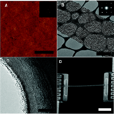
| In order to realize competitive thermoelectric devices from silicon, an approach to synthesize high-density, highly uniform nanostructures must be utilized. Recently, Tang et. al. reported on the thermoelectric performance enhancements in a new type of nanostructured material, holey silicon (HS). In their approach, the authors demonstrate nanostructured silicon membranes that exhibit ~50 times reduction in thermal conductivity as compared to non-patterned membranes of the same thickness. |
Reviewed by Jeff Morse, PhD., National Nanomanufacturing Network
Thermoelectric materials and devices convert heat to electrical power, and a variety of materials perform optimally over given temperature ranges and differentials. Significant research has been directed towards nanoscale materials and structures as a means to independently control key parameters that impact thermoelectric conversion through the suppression of thermal conductivity combined with enhancement of the electrical conductivity and Seebeck coefficient. For example, one of the more widely used thermoelectric material systems, bismuth telluride (Be2Te3), has a thermoelectric figure of merit, ZT~1 at room temperature. However, this particular material system is not widely applied to large-area energy generation due to high materials cost and low stability. For applications in energy harvesting, a lower cost, stable, more readily available material is desired. Silicon, as one example, provides an abundant, well-engineered materials platform for such applications. Porous silicon, with its randomly distributed and intertwined pore structure, has exhibited extremely low thermal conductivity, yet it suffers from low electrical conductivity as the material structure is highly deteriorated. Silicon nanowires provide another option, wherein the nanowire diameter is much smaller than the phonon mean free path or the nanowire surface is roughened to reduce thermal conductivity. For large-scale implementation however,silicon nanowires remain limited due to lack of control control over diameter and surface morphology.

Results demonstrated that the thermal conductivity of the HS membrane having 55 nm pitch was 1.14-2.03 W/m-K, a significant reduction from the 150 W/m-K exhibited by bulk silicon. The authors theorized that the reduction in thermal conductivity for the HS structures resulted from a necking effect, wherein the phonons were effectively trapped behind a hole as the silicon region bridging between the holes was significantly less than the mean free path of the phonon. In this manner, phonon transport could be suppressed while enhancing electrical conductivity of the membrane through techniques such as doping. In this manner, HS membranes having ZT~0.4 at room temperature were demonstrated for holes with 55 nm pitch. Thus it has been shown that nanostructured silicon membranes exhibit ~50 times reduction in thermal conductivity as compared to non-patterned membranes of the same thickness. The ZT parameter for these structures is independent of membrane width and provides a possible path for low-cost, large-area energy harvesting and generation from thermal sources. Additional investigations must further explore the optimization of the HS membrane for additional pore diameters and densities, as well as membrane thickness and doping.
Image reproduced with permission from Tang J, et.al., Holey Silicon as an Efficient Thermoelectric Material. Nano Letters 2010 10(10): 4279–4283. Copyright 2010 American Chemical Society.
This work is licensed under a Creative Commons Attribution-NonCommercial 3.0 Unported.
