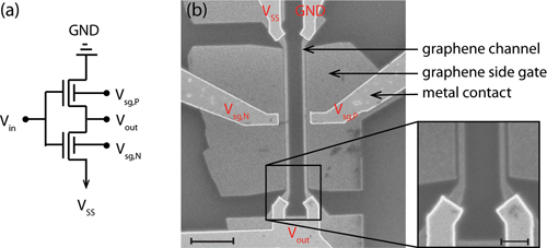
Graphene has attracted significant interest for applications in nanoelectronics resulting in its unique properties that include near ballistic electronic transport and high carrier mobility at room temperature. These properties provide potentially superior performance for both high-frequency applications, as well as for digital nanoelectronics. While a primary issue for the latter has been the lack of a semiconductor bandgap, a necessary characteristic for switching the transistor on and off which is critical for digital electronics. This issue is being addressed through innovative approaches to demonstrate a graphene inverter technology, a key building block for graphene digital circuits. This technology also has the ability to produce large area, high quality graphene at relatively low cost. While techniques including epitaxial growth and chemical vapor deposition (CVD) are being demonstrated, they remain costly or exhibit limited quality. Techniques that produce single layer graphene sheets scalable to large areas are still required.

In characterizing the anodic bonding process conditions with respect to graphene quality, the authors determined the ideal conditions were for applied voltages of 0.6-1 KV with a temperature range of 180-220°C. The authors further demonstrated that the graphene flakes could be transferred to an oxidized silicon wafer, thereby proving the basis to achieve back-gated transistor designs for device characterization. Initial measurements of materials quality and electronic properties demonstrated high carrier mobility (~6000 cm2/V-sec) and nominal high p-type doping levels on the order of 1012 cm-2. After subsequent transfer of the graphene flakes to other substrates the carrier levels were substantially reduce to ~1011 cm-2, levels that are typically observed for mechanically exfoliated graphene flakes. Thus, as innovations are made to realize novel graphene transistor circuit configurations for digital electronics, similar progress towards high yield production of quality graphene substrates are being demonstrated. While further scaling and quality control is required, major steps have been demonstrated utilizing different production techniques, each with potential benefits and potential challenges.
Reviewed by Jeff Morse, PhD, National Nanomanufacturing Network
- Moldt T, Eckmann A, Klar P, Morozov SV, Zhukov AA, Novoselov KS, Casiraghi C. 2011. High-Yield production and transfer of graphene flakes obtained by anodic bonding. ACS Nano. 5(10): 7700-7706. http://dx.doi.org/10.1021/nn202293f
Figure reprinted from Chen HY and Appenzeller J. 2011. Complementary-type graphene inverters operating at room temperature. ECE Department and Birck Nanotechnology Center, Purdue University. http://www.purdue.edu/newsroom/research/2011/110906AppenzellerGraphene.html Permission pending.
