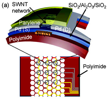
Flexible electronics are receiving significant attention for enabling a broad range of new applications and markets otherwise not possible with conventional silicon integrated circuit technology. Specifically in the areas of integrated electronics and sensors, thin-film transistors (TFTs) formed utilizing a range of nanomaterials now appear to be a viable competitor to more conventional TFT technologies such as amorphous silicon. The benefit of utilizing nanomaterials for active devices is the semiconducting properties of the specific nanomaterials. They can be optimized either during or after synthesis, then integrated into the thin-film device process sequence as a solution-based coating step. This enables the carrier transport properties of the nanomaterials to be optimized independently of device design and integration, and also provides a versatile means for adapting TFT circuit designs for flexible electronics applications. These include highly semiconductor enriched single wall carbon nanotubes (SWNTs) which are now being commercialized with >99% purity, and a range of semiconducting nanowire materials that have demonstrated charge mobility comparable to that of crystalline semiconductors. A key nanomanufacturing challenge is to maintain the performance of the individual nanoelements for the integrated system. As such many researchers have been focusing on the scaled processing of nanomaterial enhanced TFT devices and systems.

As one application example, the authors demonstrated a touch sensor integrating the SWNT TFT backplane array with a pressure-sensitive rubber. The back-plane performance further demonstrates potential as backplanes for flexible displays and touch screens. Thus, not only have high-performance TFT arrays and devices been demonstrated in which the active device layer was solution-cast, but additionally, a scaled backplane has been integrated exhibiting remarkable uniformity and consistency when subjected to a range of physical and mechanical rigors. Such an approach has significant potential to transform active matrix TFT technology as we now know it. Further process integration improvements must extend the use of facile solution-based processes to other components in the TFT device, including electrodes and gate dielectrics.
Reviewed by Jeff Morse, PhD, National Nanomanufacturing Network
- Takahashi T, Kuniharu T, Gillies AG, Fearing RS, Javey A. 2011. Carbon nanotube active-matrix backplanes for conformal electronics and sensors. Nano Letters. 11(12): 5408-5413. http://dx.doi.org/10.1021/nl203117h
Figure reprinted with permission from Takahashi T, Kuniharu T, Gillies AG, Fearing RS, Javey A. Carbon nanotube active-matrix backplanes for conformal electronics and sensors. Nano Letters. 11(12): 5408-5413. Copyright 2011 American Chemical Society.
