
In 2004, a single layer of graphite known as graphene was synthesized for the first time via mechanical exfoliation of graphite. This discovery, for which Novoselov and Geim were awarded the Nobel Prize in Physics in 2010, has ushered in a 'graphene frontier' with worldwide interest in exploiting their intriguing potential for technological applications in fields such as nanoelectronics and energy storage. The primary method that is used to fabricate large-scale transparent graphene films is chemical vapor deposition (CVD). However, this requires high-temperature processing and relatively long deposition times. Furthermore, this precludes the deposition of graphene onto temperature-sensitive substrates. Although the deposited films may be flaked off the metallic (usually Cu) substrate for transfer to another surface, this will lead to the incorporation of impurities and structural defects.
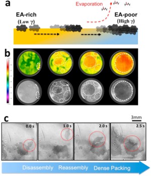
Rather than expensive vapor deposition techniques, it would be most desirable to deposit graphene films from solution suspensions. This would also allow one to deposit graphene films onto flexible surfaces, as well as low-melting substrates such as plastics. However, this strategy has only been possible using aqueous dispersions of < 5 wt% surface-functionalized graphenes due to the lack of solubility of the pristine material in solvents. In a giant leap forward, the recent report by Shin et al. (Nano Lett. 2014, ASAP; 10.1021/nl404446f) shows that rapid, inexpensive solution processing of pristine graphene films has become a reality. Their simple procedure consists of suspending the graphene platelets in a dilute (0.05 mg/mL) N-methyl-2-pyrrolidone (NMP) aqueous solution, followed by the addition of ethyl acetate (EA). Interestingly, if the NMP suspension is allowed to stand for more than two minutes without EA addition, the graphene flakes form a bulk precipitate rather than assembling into a highly uniform film on the liquid surface. The film deposition phenomenon in this system is due to the high volatility of the EA solvent. Its rapid evaporation causes the formation of convection currents that transport graphene flakes to the surface where they laterally self-assemble into uniform sheets. Using graphene flakes with diameters of 1-5 mm and 2-3 layers thick, the resultant films were typically of the same thickness (ca. 1 nm), and were easily transferred onto a variety of nonplanar substrates.
Perhaps most noteworthy about this precedent is that the simple one-step procedure works for other types of low-dimensional carbonaceous nanostructures, such as fullerenes and carbon nanotubes. These materials are also notoriously difficult to prepare as thin films in their pristine (non-functionalized) forms. By varying the solvent combinations based on the surface polarity of the nanomaterials, it is likely that this technique could also be applied to quantum dots or other inorganic-based nanomaterials. Although this technique works well in a small (8-cm diameter) batch-style system, it is not clear if/how this could be scaled up - a feature for which vapor deposition techniques are especially well-suited. Scale-up via continuous processing is an essential attribute that must be accomplished if this technique is to successfully meet the future commercial demands of graphene films for applications in advanced flexible displays, microelectronic devices, sensors, batteries/supercapacitors, photovoltaics, membranes, etc.
References:
Two-Minute Assembly of Pristine Large-Area Graphene Based Films, Jongwon Shim, Je Moon Yun, Taeyeong Yun, Pilnam Kim, Kyung Eun Lee, Won Jun Lee, Ryong Ryoo, David J. Pine, Gi-Ra Yi, and Sang Ouk Kim Nano Letters Article ASAP, DOI: 10.1021/nl404446f
Image reprinted with permission from Two-Minute Assembly of Pristine Large-Area Graphene Based Films, Jongwon Shim, Je Moon Yun, Taeyeong Yun, Pilnam Kim, Kyung Eun Lee, Won Jun Lee, Ryong Ryoo, David J. Pine, Gi-Ra Yi, and Sang Ouk Kim Nano Letters Article ASAP. Copyright 2014 American Chemical Society.