| Email not displaying correctly? View it in your browser. |
 Volume
2 Issue 11 - December 2009
Volume
2 Issue 11 - December 2009 |
|
The NNN Newsletter
Carbon Nanotube Thin Film Transistors—Ready for Prime Time?
Single walled carbon nanotubes (SWCNT) have gained significant attention over the past decade due to potentially superior electronic, mechanical, and chemical properties. For nanoelectronic applications, transistors fabricated from individual SWCNTs exhibit very high carrier mobility, yet have limited current carrying ability due to their nanoscale size. Furthermore, practical approaches to fabricate large scale integrated circuits have not yet been realized. In contrast, TFT applications simply require sufficient device characteristics (Ion/Ioff ratio, maximum current, and carrier mobility) in a thin, nominally transparent design configuration and can be fabricated by low-cost, scalable processes. Progress in device synthesis has been limited by the chirality properties of the SWCNT networks, which typically contain a mixture of semiconducting and metallic CNTs. As the SWCNTs are assembled in an overlapping configuration between the source and drain of the transistor, percolation transport through metallic nanotubes limits the device on/off ratio, yet enables high current handling capability. Rigorous purification processes have been used to yield SWCNT networks composed primarily of semiconducting nanotubes. A handful of studies published within the last year have focused on the process of integrating SWCNT networks into TFTs with very positive outcomes for industrial scale up. The knowledge gained from this nanomanufacturing research has provided sufficient progress suggesting these approaches may be suitable for rigorous process scale-up for specific applications. With key metrics for TFT devices being demonstrated, applications realizing an immediate benefit from this manufacturing approach include displays, lighting, and electronic paper. This month we take a closer look at three key papers in this area that have fostered significant interest within the community. Regards, Learn More about the Nanomaterial Enabled Conductive Paper: A New Paradigm for Flexible Electronics and Energy Storage
Working Group Makes Important Contribution to EPA's Scientific Advisory Panel on Nanosilver
Herr and Caprio Round Out Editorial Team
|
Upcoming Events December 18 - 19, 2009 December 21 - 23, 2009 December 28 - 30, 2009 January 3 - 8, 2010 January 17 - 22, 2010 January 23 - 28, 2010
Advertisement
Advertisement Affiliated Centers Recently Published Wetting 101 Degrees Wetting and Superhydrophobicity Formation and Size Tuning of Colloidal Microcapsules via Host-Guest Molecular Recognition at the Liquid-Liquid Interface 2,5-Dichlorothiophene 1,1-dioxide Nitrogen Dioxide Vapor Detection Using Poly-O-Toluidine Measuring the Structure of Epitaxially Assembled Block Copolymer Domains with Soft X-Ray Diffraction
|
|
The National Nanomanufacturing Network Newsletter Subscribe / Unsubscribe from this list. Our mailing address is: The National Nanomanufacturing Network 322 Lederle Graduate Research Center 710 N. Pleasant Street University of Massachusetts Amherst, MA 01003 Our email address is: nnn@nanomanufacturing.org Our phone number is: (413) 577-0570 Copyright (C) 2008 The National Nanomanufacturing Network All rights reserved. Supported by the National Science Foundation under Grant No. DMI-0531171. |
|
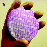 Recent efforts to synthesize carbon nanotube networks in a transistor integration strategy have shown significant promise as an alternative technology for large area TFT applications. With new knowledge of necessary process control mechanisms and carbon nanotube network properties, these approaches use solution-based assembly techniques to achieve specific device parameters by design and have the potential to gain a foothold in a high-end consumer products markets.
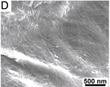 While
nanostructured materials combined with emerging nanomanufacturing
processes are advancing the next generation of displays, e-paper,
renewable energy, and energy storage devices, the predominant technologies
have employed scaled processes on flexible substrates facilitated
by roll-to-roll platforms. Recently, a group of researchers at Stanford
University have taken this concept one step further by demonstrating
the core materials and processes for fabrication of such devices
on everyday paper. Hu et. al. from Yi Cui’s research group in Stanford’s
Materials Science and Engineering Department reported their investigation
of of single walled carbon nanotubes (SWCNTs) dispersed in inks
to create high conductivity electrodes on regular paper.
While
nanostructured materials combined with emerging nanomanufacturing
processes are advancing the next generation of displays, e-paper,
renewable energy, and energy storage devices, the predominant technologies
have employed scaled processes on flexible substrates facilitated
by roll-to-roll platforms. Recently, a group of researchers at Stanford
University have taken this concept one step further by demonstrating
the core materials and processes for fabrication of such devices
on everyday paper. Hu et. al. from Yi Cui’s research group in Stanford’s
Materials Science and Engineering Department reported their investigation
of of single walled carbon nanotubes (SWCNTs) dispersed in inks
to create high conductivity electrodes on regular paper.  On November 3 – 6, 2009 the US Environmental Protection Agency (EPA) held a Scientific Advisory Panel (SAP) meeting in Arlington, Virginia to discuss the “Evaluation of Hazard and Exposure Associated with Nanosilver and Other Nanometal Oxide Pesticide Products.” Over seventy-five people from industry, regulatory, public interest, and academic sectors attended the meeting over three days. The EPA received presentations and comments from the SAP panel members during the course of the meeting, as well as six presentations during the Public Comment period. One group—The Silver Nanotechnology Working Group (SNWG)—made a detailed presentation supporting a fundamental regulatory consideration previously overlooked by many in attendance: nanosilver has been rationally manufactured, regulated, and used commercially for over a century with no significant adverse environmental, health, and safety effects.
  The National Nanomanufacturing Network is pleased to welcome two additional Contributing Editors who will round out the NNN's Editorial Team for 2010. Daniel Herr and Vincent Caprio will bring their expertise to bear on Advanced Processes + Tools and Business + Entrepreneurship focus areas for InterNano.