|
The NNN Newsletter
Commercialization
of Emergent Nanomanufacturing Platforms: Establishing Synergies
and Roadmaps
 A critical dimension of nanomanufacturing is how to address the numerous technological, economic, and regulatory challenges for scaling nanoscience developments in the research laboratory into commercializable, value-added market products. Various approaches have proven effective in fostering such transitions, including corporate and venture investments, industry consortia collaborations, private-public partnerships, and technology transfer collaborations wherein academic institutions or small businesses work with large companies to expedite the transition of technologies to mainstream applications. Although several successful prototype products and demonstrations of advanced processes exist, the outcomes for many have yet to be adopted by main stream markets and manufacturing infrastructure. A critical dimension of nanomanufacturing is how to address the numerous technological, economic, and regulatory challenges for scaling nanoscience developments in the research laboratory into commercializable, value-added market products. Various approaches have proven effective in fostering such transitions, including corporate and venture investments, industry consortia collaborations, private-public partnerships, and technology transfer collaborations wherein academic institutions or small businesses work with large companies to expedite the transition of technologies to mainstream applications. Although several successful prototype products and demonstrations of advanced processes exist, the outcomes for many have yet to be adopted by main stream markets and manufacturing infrastructure.
A significant barrier to wide-spread adoption is the cost and difficulty of supplanting existing manufacturing capabilities and platforms, thereby limiting investment in the manufacture of nanotechnology-enabled products to high value products having no alternative pathways. Consequently, many emerging nano-enabled products, tools, and materials are achieving pilot scale commercialization. A crucial next step for nanomanufacturing is to overcome the hurdles to mass production for sustainable markets.
More...
Regards,
Jeff Morse, Managing Director,
National Nanomanufacturing Network
Learn More about the 
|
NNN Test Bed Reviews February 2010
NSF Center for Hierarchical Manufacturing (CHM),
University of Massachusetts Amherst
 Hierarchical Metal Oxide Films Hierarchical Metal Oxide Films
Patterned metal oxide films having well-defined order and morphology are essential device layers in microelectronics, photovoltaics, and microfluidics for separations and sensors. In a typical fabrication process sequence, a planar metal oxide film is deposited, coated with multi-layer resist structures, patterned by optical lithography, etched, stripped, ashed, and cleaned to generate a patterned oxide film. This cycle often consists of 10 or more process steps. Moreover, the resolution of current lithography and etch techniques limit the minimum feature size precluding the direct fabrication of complex geometric structures. More....
|
NNI 2011 Budget and Signature Initiatives
 The National Nanotechnology Initiative has released its 2011 Supplement to the President's Budget. In his introductory letter, Presidential Science and Technology Advisor John Holdren notes that "Nanotechnology R&D constitutes a core building block of innovation that will ultimately accelerate job creation and transform many sectors of our economy through commercialization." The NNI budget continues to grow, with $1,701 M reported in 2009 and $1.781 M estimated for 2010. The 2011 request is slightly less - $1,762 M - but is likely to be exceeded when next year's estimates appear. In addition, the identification of three signature initiatives in areas that are "ripe for significant advances through close � interagency collaboration" gives us a glimpse of future plans, although few program details are presently available. The topics are nanoelectronics, sustainable nanomanufacturing, and solar energy. More... The National Nanotechnology Initiative has released its 2011 Supplement to the President's Budget. In his introductory letter, Presidential Science and Technology Advisor John Holdren notes that "Nanotechnology R&D constitutes a core building block of innovation that will ultimately accelerate job creation and transform many sectors of our economy through commercialization." The NNI budget continues to grow, with $1,701 M reported in 2009 and $1.781 M estimated for 2010. The 2011 request is slightly less - $1,762 M - but is likely to be exceeded when next year's estimates appear. In addition, the identification of three signature initiatives in areas that are "ripe for significant advances through close � interagency collaboration" gives us a glimpse of future plans, although few program details are presently available. The topics are nanoelectronics, sustainable nanomanufacturing, and solar energy. More...
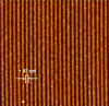
Two Approaches to Large-Area Graphene Synthesis For Device Quality Materials
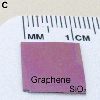 Graphene has been attracting considerable interest in recent years as a result of its unique band structure and physical properties, including extremely high carrier mobility, that make it a promising material for the semiconductor industry, though not one without challenges. One issue to consider has been the methods used to produce graphene films, including exfoliated graphite which yields graphene sheets sufficient only for research studies. Recent approaches to large-area synthesis of high quality single layer and multilayer graphene films have been explored by thermal decomposition of single crystal silicon carbide and chemical vapor deposition (CVD) on single crystal transition metals. While these approaches represent a significant step towards scaled production of quality graphene films, the requirements of high vacuum processing and expensive substrates with limited size still fall short of an integrated approach to incorporate this materials system.More.... Graphene has been attracting considerable interest in recent years as a result of its unique band structure and physical properties, including extremely high carrier mobility, that make it a promising material for the semiconductor industry, though not one without challenges. One issue to consider has been the methods used to produce graphene films, including exfoliated graphite which yields graphene sheets sufficient only for research studies. Recent approaches to large-area synthesis of high quality single layer and multilayer graphene films have been explored by thermal decomposition of single crystal silicon carbide and chemical vapor deposition (CVD) on single crystal transition metals. While these approaches represent a significant step towards scaled production of quality graphene films, the requirements of high vacuum processing and expensive substrates with limited size still fall short of an integrated approach to incorporate this materials system.More....
Read more on 
|
Upcoming Events
March 7 - 10, 2010
Surface Analysis 2010
March 7 - 11, 2010
SPIE Smart Structures/NDE
March 9 - 12, 2010
NanoImpactNet Lausanne 2010
March 21 - 25, 2010
ACS Spring 2010 National Meeting and Exposition
March 24 - 25, 2010
Nanocomposites and Nanotubes 2010
Advertisement

Upcoming Calls
March 19, 2010
Nanotoxicology 2010
Deadline to submit abstracts
April 17, 2010
Nanosens 2010
Deadline to submit poster abstracts
May 4, 2010
Greener Nano 2010
Deadline to submit poster abstracts
May 18, 2010
International Conference on Green Remediation
Deadline to submit abstracts
May 22, 2010
Gordon Research Conference: Plasmonics
Deadline to apply to attend
Advertisement

Recently Published
From Our Affiliates
Ultralyophobic Oxidized Aluminum Surfaces Exhibiting Negligible Contact Angle Hysteresis
Langmuir 26(4): 2567-2573
Formation of SiO2 Air-Gap Patterns Through scCO(2) Infusion of NIL Patterned PHEMA
Chemistry of Materials 22(4): 1445-1451
Laser Desorption/Ionization Mass Spectrometry Analysis of Monolayer-Protected Gold Nanoparticles
Analytical and Bioanalytical Chemistry 396 (3): 1025 - 1035
Advertisement

Affiliated Centers


|
 Volume
3 Issue 2 - February 2010
Volume
3 Issue 2 - February 2010