|
The NNN Newsletter
Challenges Remain for Effective Growth of Nanotechnology Enabled Products
 The investment made by the federal government via the National Nanotechnology Initiative (NNI) to spawn growth of emerging nano-enabled products and maintain global leadership by the U.S. in fundamental nanoscale science and technology has been effective in meeting specified goals and objectives over the first decade. According to conclusions from the recent report by the President's Council of Advisors on Science and Technology (PCAST) the $12B NNI investment in nanotechnology since 2001 has provided a "catalytic and substantial impact." Yet, with this positive assessment, significant challenges remain in order to stimulate sustainable economic impact and growth through commercialization of nanotechnologies. These challenges include workforce training and education while further balancing key issues of societal impact and worker safety through regulatory oversight. Several issues have recently been cited by industry groups, government organizations, and the PCAST report regarding regulation, workforce training, and effective commercialization of nanoscience breakthroughs that suggest a critical balance must be struck during the second decade of the NNI in order to optimally reap the benefits of federal investments. The investment made by the federal government via the National Nanotechnology Initiative (NNI) to spawn growth of emerging nano-enabled products and maintain global leadership by the U.S. in fundamental nanoscale science and technology has been effective in meeting specified goals and objectives over the first decade. According to conclusions from the recent report by the President's Council of Advisors on Science and Technology (PCAST) the $12B NNI investment in nanotechnology since 2001 has provided a "catalytic and substantial impact." Yet, with this positive assessment, significant challenges remain in order to stimulate sustainable economic impact and growth through commercialization of nanotechnologies. These challenges include workforce training and education while further balancing key issues of societal impact and worker safety through regulatory oversight. Several issues have recently been cited by industry groups, government organizations, and the PCAST report regarding regulation, workforce training, and effective commercialization of nanoscience breakthroughs that suggest a critical balance must be struck during the second decade of the NNI in order to optimally reap the benefits of federal investments.
The top recommendations of the PCAST report include increasing investments in nanomanufacturing and product commercialization to facilitate the entrance of novel nanotech products into the marketplace, while also growing the workforce with expertise in nanofabrication and strengthening commitments to environmental, health, and safety (EHS) research. Additional recommendations included an increase in the NNI investment in nanomanufacturing by 100% over the next five years. In 2011, government funding for nanomanufacturing is proposed to make up only 5.8% of the total NNI budget.
More...
Regards,
Jeff Morse, Managing Director,
National Nanomanufacturing Network
Learn More about the 
Understanding the Resistivity-Transparency Tradeoffs for Carbon Nanotube Electrodes on Flexible Substrates
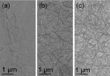 Transparent electrodes suitable for flexible substrates are a critical element of numerous technologies including solar photovoltaics (PV), displays, and organic light emitting diodes. At present indium tin oxide (ITO) is the predominant material used for these applications. The drawback of ITO is its limited supply, which has driven up cost in recent years, along with the brittleness of the materials system that makes it problematic for flexible applications. As such, a significant amount of research has focused on identifying alternative materials to replace ITO. Carbon nanotubes (CNTs) have drawn a lot of attention due to their high electronic conductivity, low cost, and suitability to form solvent ink dispersions that can be spin or spray coated. The varying levels of conductivity for CNT films has been mainly attributed to the solvent formulations and subsequent acid washing chemistries that can either leave a residue on the CNTs, which acts as a barrier to electron conduction, or damage the CNTs themselves. Progress in this area has resulted in reductions in sheet resistance of films formed from suitable dispersions to the point where CNT electrodes are now competitive for next generation products on flexible substrates. More.... Transparent electrodes suitable for flexible substrates are a critical element of numerous technologies including solar photovoltaics (PV), displays, and organic light emitting diodes. At present indium tin oxide (ITO) is the predominant material used for these applications. The drawback of ITO is its limited supply, which has driven up cost in recent years, along with the brittleness of the materials system that makes it problematic for flexible applications. As such, a significant amount of research has focused on identifying alternative materials to replace ITO. Carbon nanotubes (CNTs) have drawn a lot of attention due to their high electronic conductivity, low cost, and suitability to form solvent ink dispersions that can be spin or spray coated. The varying levels of conductivity for CNT films has been mainly attributed to the solvent formulations and subsequent acid washing chemistries that can either leave a residue on the CNTs, which acts as a barrier to electron conduction, or damage the CNTs themselves. Progress in this area has resulted in reductions in sheet resistance of films formed from suitable dispersions to the point where CNT electrodes are now competitive for next generation products on flexible substrates. More....
NanoBusiness Alliance Interview with Ajay Malshe
Ajay P. Malshe is the Co-founder and Chief Technology Officer of NanoMech LLC. NanoMech LLC is a nanotechnology innovations platform company with major current nanomanufacturing and product foci in four application sectors. These sectors are Machining (ex. TuffTek®) and Lubrication (NanoGlideTM), Sustainable Retail Packaging (Guard-In-FreshTM), Biomedical and Defense. NanoMech is creating world class innovations and innovations based hi-tech job opportunities in Arkansas and US, at large. In this interview, Steve Waite talks to Ajay Malshe about NanoMech and his vision for nanotech in the decade ahead. More....
NIST Wins R&D100 Award for Through-focus Scanning Optical Microscopy
 Ravikiran Attota, a lead researcher in the National Institute for Standards and Technology 's Precision Engineering Division, has been awarded a 2010 R&D100 Award in the Microscopy category for his development of Through-focus Scanning Optical Microscopy (TSOM), a method which transforms conventional optical microscopes into 3D metrology tools with nanometer sensitivity. TSOM allows a user to analyze samples from multiple image planes along the focus direction, instead of the typical analysis from a single plane. It collects 2-D images at different focal positions from a conventional bright field optical microscope, extracts brightness profiles from these multiple out-of-focus images, and uses the differences between them to construct the TSOM image. More.... Ravikiran Attota, a lead researcher in the National Institute for Standards and Technology 's Precision Engineering Division, has been awarded a 2010 R&D100 Award in the Microscopy category for his development of Through-focus Scanning Optical Microscopy (TSOM), a method which transforms conventional optical microscopes into 3D metrology tools with nanometer sensitivity. TSOM allows a user to analyze samples from multiple image planes along the focus direction, instead of the typical analysis from a single plane. It collects 2-D images at different focal positions from a conventional bright field optical microscope, extracts brightness profiles from these multiple out-of-focus images, and uses the differences between them to construct the TSOM image. More....
Read more on  |
Upcoming Events
August 1 - 5, 2010
SPIE Nanoscience + Technology
August 4, 2010
Delivering on the Promise of Carbon Nanotube Technology in Industry
August 8 - 13, 2010
Gordon Research Conference: Magnetic Nanostructures
August 15 - 19, 2010
International Materials Research Congress 2010
August 17 - 20, 2010
Nano Korea / IEEE Nano 2010
View Full Calendar
Advertisement

Upcoming Calls
August 30, 2010
BIT's 1st Annual World Congress of Nanomedicine
Deadline for poster abstracts
September 14, 2010
IEEE Nanosensors 2010
Open Poster Program Submission Deadline
September 15, 2010
Nanoinformatics 2010
Deadline for papers and poster abstracts
Recently Published
From Our Affiliates
Tuning Payload Delivery in Tumor Cylindroids Using Gold Nanoparticles
Nature Nanotechnology 5(6):465-472
Toxicity of Carbon Nanotubes to the Activated Sludge Process
Journal of Hazardous Materials 178(1-3):356-362
Effect of Different Deposition Mediums on the Adhesion and Removal of Particles
Journal of the Electrochemical Society 157(6):H662-H665
Controlled Alignment of Multiple Proteins and Nanoparticles with Nanometer Resolution via Backbone-Modified Phosphorothioate DNA and Bifunctional Linkers
Journal of the American Chemical Society 132(26):8906+
Study of a High Performance AFM Probe-Based Microscribing Process
Journal of Manufacturing Science and Engineering-Transactions of the ASME 132(3):030906
Affiliated Centers


|
 Volume
3 Issue 7 - July 2010
Volume
3 Issue 7 - July 2010