|
The NNN Newsletter
Emerging Nanomanufacturing Techniques Included on Industry Roadmaps
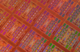 Significant challenges exist for nanomanufacturing processes to gain acceptance within various industries, due in part to a mature infrastructure and supply chain, as well as potentially high capital expenses for technologies that might supplant existing tools and processes. While these issues are present in most sectors, the semiconductor industry is an prime example of an area where critical need must be demonstrated to justify the costs of replacing a substantial existing infrastructure. For example, optical lithographic tools enable patterning techniques that will only carry the industry for a few more years, after which no proven optical solutions exist to maintain progress within the constraints of the present roadmap. As a result, the International Technology Roadmap for Semiconductors (ITRS, 2009) includes both nanoimprint and directed self-assembly (DSA) patterning as part of the future roadmap for patterning solutions. Significant challenges exist for nanomanufacturing processes to gain acceptance within various industries, due in part to a mature infrastructure and supply chain, as well as potentially high capital expenses for technologies that might supplant existing tools and processes. While these issues are present in most sectors, the semiconductor industry is an prime example of an area where critical need must be demonstrated to justify the costs of replacing a substantial existing infrastructure. For example, optical lithographic tools enable patterning techniques that will only carry the industry for a few more years, after which no proven optical solutions exist to maintain progress within the constraints of the present roadmap. As a result, the International Technology Roadmap for Semiconductors (ITRS, 2009) includes both nanoimprint and directed self-assembly (DSA) patterning as part of the future roadmap for patterning solutions.
More...
Regards,
Jeff Morse, Managing Director,
National Nanomanufacturing Network
Learn More about the 
|
This Week
Nanotechnology Long-term Impacts and Research Directions: 2000-2020
Webcast
At the behest of the National Science Foundation (NSF), the World Technology Evaluation Center, Inc. (WTEC) conducted an international study involving 200 leading experts from 35 countries that synthesized progress in nanotechnology over the last decade as well as future directions for nanotech. The study's findings--highlighted in a new report, Nanotechnology Long-term Impacts and Research Directions: 2000-2020--will be released during a webcast workshop on Sept. 30 from 8:30 a.m. to 4:00 EDT. A draft report will be posted for public comment from September 30 to October 15, 2010. To view the webcast, access the website and provide your email address.
NSF Press Release 9/23/10 Workshop Web site
|
Aligned Carbon Nanotube Patterning Via Dry Contact Transfer Printing
 Techniques to align CNT networks in-plane on a substrate have been investigated as a means to enable CNT-based electronic devices including transistors ad interconnects. One approach—transferring CNT thin films from one surface to another via a soft lithography—suffers from limited ability to achieve good adhesion of the CNT films to the transfer substrate and imprecise alignment of the CNT patterns. Ultimately, a transfer technique that can be scaled to large area with high throughput processing at low temperature is required to achieve flexible substrates for many emerging display, lighting, and solar PV applications. Pint et. al. report a scalable means to create aligned CNT thin film patterns on both rigid and flexible substrates. More.... Techniques to align CNT networks in-plane on a substrate have been investigated as a means to enable CNT-based electronic devices including transistors ad interconnects. One approach—transferring CNT thin films from one surface to another via a soft lithography—suffers from limited ability to achieve good adhesion of the CNT films to the transfer substrate and imprecise alignment of the CNT patterns. Ultimately, a transfer technique that can be scaled to large area with high throughput processing at low temperature is required to achieve flexible substrates for many emerging display, lighting, and solar PV applications. Pint et. al. report a scalable means to create aligned CNT thin film patterns on both rigid and flexible substrates. More....
NCMS Releases Findings from 3rd Study of Nanotechnology in the U.S. Manufacturing Industry
 The National Center for Manufacturing Sciences has released the report from its third, NSF-funded, nation-wide survey gauging the momentum of nanotechnology develoment and depoloyment in the U.S. manufacturing industry. The survey targeted senior executives in U.S.-based manufacturing and research organizations and addressed pre-competitive and strategic issues influencing their organizations' nanotechnology commercialization initiatives. The goals of the survey were to identify and highlight trends in nanotechnology tech transfer and to make recommendations to accelerate product development and competitiveness. More.... The National Center for Manufacturing Sciences has released the report from its third, NSF-funded, nation-wide survey gauging the momentum of nanotechnology develoment and depoloyment in the U.S. manufacturing industry. The survey targeted senior executives in U.S.-based manufacturing and research organizations and addressed pre-competitive and strategic issues influencing their organizations' nanotechnology commercialization initiatives. The goals of the survey were to identify and highlight trends in nanotechnology tech transfer and to make recommendations to accelerate product development and competitiveness. More....
NanoBusiness Alliance Interview with Larry Bock
 Steve Waite talks to Larry Bock about the state of science and engineering in the United States and what he and his organization are doing to help keep the spirit of science and engineering-driven innovation alive and well in America. Larry is a successful serial entrepreneur who has founded, co-founded or financed the early stage growth of 40 companies in the life and physical sciences from inception to achieving an aggregate market capitalization in excess of $30 Billion. Larry is a Special Limited Partner and currently serves as Chairman of Lux Ventures' Advisory Board of industry experts. Larry was a co-founder and executive chairman of Nanosys, Inc. More.... Steve Waite talks to Larry Bock about the state of science and engineering in the United States and what he and his organization are doing to help keep the spirit of science and engineering-driven innovation alive and well in America. Larry is a successful serial entrepreneur who has founded, co-founded or financed the early stage growth of 40 companies in the life and physical sciences from inception to achieving an aggregate market capitalization in excess of $30 Billion. Larry is a Special Limited Partner and currently serves as Chairman of Lux Ventures' Advisory Board of industry experts. Larry was a co-founder and executive chairman of Nanosys, Inc. More....
Read more on  |
Upcoming Events
October 6, 2010
Environmental Applications of Nanotechnology: Going Green
October 6, 2010
Large-Scale Engineered Synthesis of BaTiO3 Nanoparticles
October 13 - 15, 2010
Non-Destructive RealTime Process Control
October 17 - 22, 2010
AVS 57th International Symposium and Exhibition
October 23 - 25, 2010
BIT's 1st Annual World Congress of Nanomedicine 2010
View Full Calendar
Advertisement

Upcoming Calls
September 14, 2010
IEEE Nanosensors 2010
Open Poster Program Submission Deadline
October 15, 2010
Nanoinformatics 2010
Deadline for papers and poster abstracts
Recently Published
From Our Affiliates
High-speed and Drop-on-demand Printing with a Pulsed Electrohydrodynamic Jet
Journal of Micromechanics and Microengineering 20(9): 095026
Performance of Ultrathin Silicon Solar Microcells with Nanostructures of Relief Formed by Soft Imprint Lithography for Broad Band Absorption Enhancement
Nano Letters 10(8):3041-3046
Comparison of Label-free Biosensing in Microplate, Microfluidic, and Spot-based Affinity Capture Assays
Analytical Biochemistry 405(1): 1-10
Light Emission Characteristics and Mechanics of Foldable Inorganic Light-Emitting Diodes
Advanced Materials 22(28): 3062-3066
Image force microscopy of molecular resonance: A microscope principle
Applied Physics Letters 97(7): 073121
Affiliated Centers


|
 Volume
3 Issue 9 - September 2010
Volume
3 Issue 9 - September 2010