|
Advanced Manufacturing Partnership: Where Does Nanomanufacturing Fit, and Where Should Investments Be Made?
The announcement of the Advanced Manufacturing Partnership (AMP) by the White House last June, followed by regional workshops to identify technology approaches for U.S. government investment to create high-quality manufacturing jobs and enhance the global competitiveness, demonstrates the Obama administration's commitment to revitalizing manufacturing in the US. The government/academic/industry AMP collaboration convened the workshops to exchange ideas between the AMP steering committee and stakeholders including entrepreneurs, manufacturing leaders, public officials, educators, students and the general public on how best to make it in America. Topics for discussion included technology development, education, workforce development, and shared infrastructure and facilities. The AMP steering committee heard from private sector leaders representing a wide range of manufacturing sectors and global corporations, as well as from federal and state policymakers. In evaluating the Advanced Manufacturing Partnership and the intended impact towards a sustainable and growing manufacturing base in the U.S., several aspects of the dialogue provide encouragement while quantifying the magnitude of the challenges faced. For example, workforce training at the high school and junior college levels includes new curricula and strategies, yet still faces the challenge of reinvigorating the perception of manufacturing careers for future generations. Many states have already established and begun execution of roadmaps and efforts in this area. More....
Regards,
National Nanomanufacturing Network
Learn More about the 
Integrated Nanowire Logic Circuitry on Deformable Nonplanar Substrates
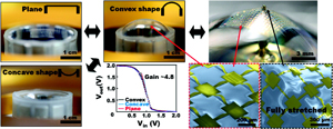 While a significant amount of recent research and development has focused on flexible electronics and improvements in thin film transistor performance on flexible substrates, less attention has been given to electronics application requiring deformable layouts or extreme, complex surface shapes and curvatures. As flexible electronics technology matures, a growing number of applications require stretchable or extreme nonplanar systems approaches. Examples of these applications include electronic eye cameras, hemispherical or curvilinear electronics, prosthetic or medical sensors, and stretchable LEDs, displays, photovoltaics, sensors, or logic devices utilizing thin silicon. In all of these applications it is critical to maintain the performance of the active electronic devices as the substrate is deformed due to changes in shape or external applied forces. A key issue related to this is the adjustment in resistive properties of nanomaterial-elastomer composites as the elastomeric substrates is stretched, thereby necessitating different approaches for the design and manufacture of deformable electronic systems. More.... While a significant amount of recent research and development has focused on flexible electronics and improvements in thin film transistor performance on flexible substrates, less attention has been given to electronics application requiring deformable layouts or extreme, complex surface shapes and curvatures. As flexible electronics technology matures, a growing number of applications require stretchable or extreme nonplanar systems approaches. Examples of these applications include electronic eye cameras, hemispherical or curvilinear electronics, prosthetic or medical sensors, and stretchable LEDs, displays, photovoltaics, sensors, or logic devices utilizing thin silicon. In all of these applications it is critical to maintain the performance of the active electronic devices as the substrate is deformed due to changes in shape or external applied forces. A key issue related to this is the adjustment in resistive properties of nanomaterial-elastomer composites as the elastomeric substrates is stretched, thereby necessitating different approaches for the design and manufacture of deformable electronic systems. More....
NanoBusiness Interview: Jason Hartlove, CEO, Nanosys
 In this month's interview, we talk to Jason Hartlove, President & CEO of Nanosys, Inc. Jason has a track record of building and leading innovative companies and business units by driving emerging technologies from R&D to market application. Prior to joining Nanosys he was President of MagnaChip Semiconductor and was responsible for managing all business activities for the Imaging Solutions Division headquartered in Seoul, South Korea. Prior to MagnaChip, Mr. Hartlove served as Vice President and General Manager for the Sensor Solutions Division of Agilent Technologies and its parent company Hewlett-Packard. Working in collaboration with Hewlett-Packard Laboratories from 1996, he developed the first commercial implementations of optical position sensing used in optical mice and CMOS image sensor technologies for the company. Mr. Hartlove is the author of more than 20 patents, including the winner of the Hewlett Award in 2004 for best patent in Agilent Technologies. He has also worked in a variety of manufacturing, R&D and marketing roles in semiconductor technologies including MEMS, III -V, bipolar, CMOS and BCD process technologies. Mr. Hartlove holds a B.S. in electrical engineering from UCLA and has completed graduate work at the Anderson School of Management at UCLA. More... In this month's interview, we talk to Jason Hartlove, President & CEO of Nanosys, Inc. Jason has a track record of building and leading innovative companies and business units by driving emerging technologies from R&D to market application. Prior to joining Nanosys he was President of MagnaChip Semiconductor and was responsible for managing all business activities for the Imaging Solutions Division headquartered in Seoul, South Korea. Prior to MagnaChip, Mr. Hartlove served as Vice President and General Manager for the Sensor Solutions Division of Agilent Technologies and its parent company Hewlett-Packard. Working in collaboration with Hewlett-Packard Laboratories from 1996, he developed the first commercial implementations of optical position sensing used in optical mice and CMOS image sensor technologies for the company. Mr. Hartlove is the author of more than 20 patents, including the winner of the Hewlett Award in 2004 for best patent in Agilent Technologies. He has also worked in a variety of manufacturing, R&D and marketing roles in semiconductor technologies including MEMS, III -V, bipolar, CMOS and BCD process technologies. Mr. Hartlove holds a B.S. in electrical engineering from UCLA and has completed graduate work at the Anderson School of Management at UCLA. More...
Lead-Free Nanowire Piezoelectric Nanogenerator: Potential for Ubiquitous Power
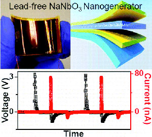 Scavenging energy from the environment at meaningful power densities remains an elusive and costly target for a range of small-scale applications, such as wireless sensors and autonomous information networks. In addition, prospects for scaling such technologies to provide real energy production from renewable sources could be a driver for such technologies, but require much more stringent cost and scaled manufacturing targets. Environmentally renewable sources of energy that scale from miniaturized power sources to large scale energy production include solar, thermal, and vibrational, all of which have been enhanced by the incorporation of nano-enabled materials and nanomanufacturing processes. In many scenarios, an ideal system might include each type of energy conversion device implemented in a thin stack with energy storage elements. As this vision gains momentum, optimization of each type of conversion element is still required, both from a materials and scaled fabrication standpoint. In the case of vibration energy scavenging, research on nanowire (NW) piezoelectric power generation has focused on the use of zinc oxide (ZnO) or ferroelectric materials (lead zirconate (PbZrO3), lead titanate (PbTiO3), barium titanate (BaTiO3)). Piezoelectric nanogenerators fabricated from these materials have demonstrated modest power densities, yet still have challenges of scalable materials processes, along with the concern of toxic materials for scaled implementations.
More.... Scavenging energy from the environment at meaningful power densities remains an elusive and costly target for a range of small-scale applications, such as wireless sensors and autonomous information networks. In addition, prospects for scaling such technologies to provide real energy production from renewable sources could be a driver for such technologies, but require much more stringent cost and scaled manufacturing targets. Environmentally renewable sources of energy that scale from miniaturized power sources to large scale energy production include solar, thermal, and vibrational, all of which have been enhanced by the incorporation of nano-enabled materials and nanomanufacturing processes. In many scenarios, an ideal system might include each type of energy conversion device implemented in a thin stack with energy storage elements. As this vision gains momentum, optimization of each type of conversion element is still required, both from a materials and scaled fabrication standpoint. In the case of vibration energy scavenging, research on nanowire (NW) piezoelectric power generation has focused on the use of zinc oxide (ZnO) or ferroelectric materials (lead zirconate (PbZrO3), lead titanate (PbTiO3), barium titanate (BaTiO3)). Piezoelectric nanogenerators fabricated from these materials have demonstrated modest power densities, yet still have challenges of scalable materials processes, along with the concern of toxic materials for scaled implementations.
More....
Read more on  |


Advertisements


Job Opportunities
Lab EHS Specialist, Safety Partners, Inc.
Faculty Position in Computer Science and Engineering, University of Illinois at Urbana-Champaign
Postdoctoral Researcher Transport Modeling of Junctionless Nanowire Transistor, Imec
Upcoming Events
Jan 20-23, 2012
International Conference on Nano Science and Technology
January 21-26, 2012
SPIE Photonics West
Feb 6-9, 2012
2012FLEX - Flexible Electronics & Displays
View Full Calendar
Upcoming Calls
Bio Nanotech 2012
Submissions accepted until December 16, 2011
SPIE Optics + Photonics 2012
Submissions accepted until January 20, 2012
SPIE NanoScience + Engineering
Submissions accepted until January 30, 2012
Graphene 2012
Submissions accepted until Februrary 10, 2012
View All Calls

Recently Published
From Our Affiliates
Multicore-Shell PNIPAm-co-PEGMa Microcapsules for Cell Encapsulation
Langmuir 27(22)
Modulating the performance of carbon nanotube field-effect transistors via Rose Bengal molecular doping
Nanotechnology 22(45)
Control of high-resolution electrohydrodynamic jet printing
Control Engineering Practice 19(11):1266-1273
Spatial Diffusion of Water in Carbon Nanotubes: From Fickian to Ballistic Motion
Journal of Physical Chemistry 115(42):12145-12149
Switching of +/- 360 degrees domain wall states in a nanoring by an azimuthal Oersted field
Nanotechnology 22(48)
Affiliated Centers


|
 Volume
4 Issue 11 - November/December 2011
Volume
4 Issue 11 - November/December 2011