|
The NNN Newsletter
New Challenges Face Nanotechnology Investments to Simultaneously Stimulate Research and Innovation
 At a time when both public and private stakeholders are evaluating the impact of the last decades' investments in nanotechnology research and development, numerous indicators provide a positive outlook for both short and long term strategies for future investments. The indicators and data providing a positive outlook for increased future opportunities are predominantly derived from the recent manufacturing report on business by the Institute of Supply Management (ISM, December 2010). From this report, the broad picture indicates that most manufacturing industry sectors have experienced some and anticipate further expansion as forecast by the purchasing managers index (PMI). Simultaneously, government, academic, and private stakeholders are assessing models and strategies for future investments in nanotechnology in order to provide sustainable growth and economic impact. In part, this is due to the fact that, while the U.S. investment under the National Nanotechnology Initiative (NNI) has clearly transformed nanoscience research over the past decade, innovation and commercialization has not kept pace. New policy and organizational strategies are clearly warranted to foster growth in innovation, and effectively facilitate the transition from laboratory science to commercialization. At a time when both public and private stakeholders are evaluating the impact of the last decades' investments in nanotechnology research and development, numerous indicators provide a positive outlook for both short and long term strategies for future investments. The indicators and data providing a positive outlook for increased future opportunities are predominantly derived from the recent manufacturing report on business by the Institute of Supply Management (ISM, December 2010). From this report, the broad picture indicates that most manufacturing industry sectors have experienced some and anticipate further expansion as forecast by the purchasing managers index (PMI). Simultaneously, government, academic, and private stakeholders are assessing models and strategies for future investments in nanotechnology in order to provide sustainable growth and economic impact. In part, this is due to the fact that, while the U.S. investment under the National Nanotechnology Initiative (NNI) has clearly transformed nanoscience research over the past decade, innovation and commercialization has not kept pace. New policy and organizational strategies are clearly warranted to foster growth in innovation, and effectively facilitate the transition from laboratory science to commercialization.
More...
Regards,
Jeff Morse, Managing Director,
National Nanomanufacturing Network
Learn More about the 
Thermoplastic Nanocomposites via Nanoinfusion Processing
 Applied Nanoinfusion Inc. (Dayton, OH) is nearing commercialization of its technology to develop and manufacture in-situ thermoplastic nanocomposites via nanoinfusion processing. Nanoinfusion processing alleviates the need for traditional nanoparticle synthesis and produces a 100% dispersed thermoplastic nanocomposite with zero nanoparticle agglomeration. The result, is the first in-situ nanocomposite, with 100% dispersion and the capability to produce mono-sized nanoparticles. Dr. Stan Prybyla, President of Applied Nanoinfusion, commented that the technology works with virtually all thermoplastics, including numerous high performance thermoplastics. More.... Applied Nanoinfusion Inc. (Dayton, OH) is nearing commercialization of its technology to develop and manufacture in-situ thermoplastic nanocomposites via nanoinfusion processing. Nanoinfusion processing alleviates the need for traditional nanoparticle synthesis and produces a 100% dispersed thermoplastic nanocomposite with zero nanoparticle agglomeration. The result, is the first in-situ nanocomposite, with 100% dispersion and the capability to produce mono-sized nanoparticles. Dr. Stan Prybyla, President of Applied Nanoinfusion, commented that the technology works with virtually all thermoplastics, including numerous high performance thermoplastics. More....
Hybrid Silicon/Carbon Nanotube Heterostructures for Reversible High-Capacity Lithium-Ion Anodes
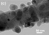 In the search for high performance lithium ion (Li+) battery systems that will provide increased energy density along with improved cycling stability, silicon has emerged as a strong candidate to replace existing graphite anode systems due its inherently high capacity (theoretical specific capacity ~4200 mAh/g). To date, the utilization of silicon anodes in Li+ battery systems has been limited by rapid capacity degradation after only a few charge-discharge cycles resulting from substantial volume expansion due to phase transitions occurring during the Lithium alloying/dealloying processes. Such volume expansions lead to a rapid decrease in reversible capacity as the silicon essentially disintegrates. Although approaches employing porous silicon, silicon nanoparticles, and silicon coated carbon nanofibers have been investigated, they have shown limited improvements in cycling stability and capacity. Therefore methods to synthesize silicon anode structures that will retain the intrinsic capacity while demonstrating long term cycling stability and reversible capacity performance are necessary. More.... In the search for high performance lithium ion (Li+) battery systems that will provide increased energy density along with improved cycling stability, silicon has emerged as a strong candidate to replace existing graphite anode systems due its inherently high capacity (theoretical specific capacity ~4200 mAh/g). To date, the utilization of silicon anodes in Li+ battery systems has been limited by rapid capacity degradation after only a few charge-discharge cycles resulting from substantial volume expansion due to phase transitions occurring during the Lithium alloying/dealloying processes. Such volume expansions lead to a rapid decrease in reversible capacity as the silicon essentially disintegrates. Although approaches employing porous silicon, silicon nanoparticles, and silicon coated carbon nanofibers have been investigated, they have shown limited improvements in cycling stability and capacity. Therefore methods to synthesize silicon anode structures that will retain the intrinsic capacity while demonstrating long term cycling stability and reversible capacity performance are necessary. More....
Atomic-Scale Metrology is Key in Fabricating Graphene Devices
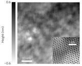 Graphene is a very interesting nanomaterial with potential for applications in many different fields including nanoelectronics. However, the properties of graphene can vary broadly and depend sensitively on its integration in device structures and the details of its interaction with other materials, such as underlying substrates or gate dielectrics. Unlike other semiconductor electronic devices, where the active layer is buried below the surface and where microscopic details of transport cannot be directly examined, graphene is exposed at a surface and can be directly examined on the atomic scale using scanning tunneling microscopy (STM) and scanning tunneling spectroscopy (STS). More.... Graphene is a very interesting nanomaterial with potential for applications in many different fields including nanoelectronics. However, the properties of graphene can vary broadly and depend sensitively on its integration in device structures and the details of its interaction with other materials, such as underlying substrates or gate dielectrics. Unlike other semiconductor electronic devices, where the active layer is buried below the surface and where microscopic details of transport cannot be directly examined, graphene is exposed at a surface and can be directly examined on the atomic scale using scanning tunneling microscopy (STM) and scanning tunneling spectroscopy (STS). More....
Read more on  |
Advertisement

Upcoming Events
January 27, 2010
Exosome Characterization by Nanoparticle Tracking Analysis
February 3, 2010
Energy Storage: Develop Competitive Strategies and Target Markets
February 7 - 10, 2010
Flex 2011
February 7 - 11, 2010
AMN-5
February 17, 2010
Rice Alliance Nanotechnology and Sustainability Venture Forum
December 5 - 8, 2010
Society for Risk Analysis Annual Meeting
View Full Calendar
Upcoming Calls
Electronic Materials Conference
Submissions accepted until January 31
SPIE NanoScience + Engineering
Deadline for abstracts February 7
IEEE Nano 2011
Deadline for abstracts March 15
View All Calls
Advertisement

Recently Published
From Our Affiliates
An Integrated Planning Approach for a Nanodeposition Manufacturing Process
International Journal of Advanced Manufacturing Technology 51(5-8):561-573
Rediscovering Silicones: Molecularly Smooth, Low Surface Energy, Unfilled, UV/Vis-Transparent, Extremely Cross-Linked, Thermally Stable, Hard, Elastic PDMS
Langmuir 26(24):18585-18590
Colloidal Microcapsules: Self-Assembly of Nanoparticles at the Liquid-Liquid Interface
Chemistry-An Asian Journal 5(12):2442-2453
Hydrogen-Bond-Mediated Phase Behavior of Complexes of Small Molecule Additives with Poly(ethylene oxide-b-propylene oxide-b-ethylene oxide) Triblock Copolymer Surfactants
Macromolecules 43(23):9990-9997
Energetics of Association in Poly(lactic acid)-based Hydrogels with Crystalline and Nanoparticle- Polymer Junctions
Langmuir 26(22):17330-17338
Affiliated Centers


|
 Volume
4 Issue 1 - January 2011
Volume
4 Issue 1 - January 2011