|
The NNN Newsletter
The Nanomanufacturing Revolution and Continuing Impact: Nanomanufacturing Summit 2011
 As the impact of public and private sector investments in nanotechnology for more than a decade now continues to evolve, we are moving into a new era whereby a decade of intense scientific research gives way to fundamentally new products that will have significant societal and economic impact. As the predicted billions and trillions of dollars of emerging nano-enabled products enter the marketplace, the interest and focus on nanomanufacturing and the commercialization of nanotechology will grow. Nanomanufacturing processes previously considered fundamental science are now key enablers to solve critical issues in the evolution of many products, fueling the innovation cycle to realize completely new products. These processes include bottom-up directed assembly, top-down high-resolution patterning and manipulation, molecular and biological systems engineering, and hierarchical integration across multiple length scales. As the impact of public and private sector investments in nanotechnology for more than a decade now continues to evolve, we are moving into a new era whereby a decade of intense scientific research gives way to fundamentally new products that will have significant societal and economic impact. As the predicted billions and trillions of dollars of emerging nano-enabled products enter the marketplace, the interest and focus on nanomanufacturing and the commercialization of nanotechology will grow. Nanomanufacturing processes previously considered fundamental science are now key enablers to solve critical issues in the evolution of many products, fueling the innovation cycle to realize completely new products. These processes include bottom-up directed assembly, top-down high-resolution patterning and manipulation, molecular and biological systems engineering, and hierarchical integration across multiple length scales.
The impact of nanomanufacturing has already begun to be realized with examples that include directed self-assembly (DSA) for high-density bit patterned data storage media, the inclusion of DSA in the roadmap for the semiconductor industry, and the scaled production of nanocomposites and nanomaterials via both new and existing manufacturing infrastructure. Nanostructured materials such as carbon nanotubes, graphene, and a range of nanoparticle materials have achieved new levels of performance for applications such as transparent electrodes, thin film transistors, next generation electronics, energy storage, nanomedicine, renewable energy, and resource remediation. This range of nano-enabled products represents both significant markets as well as critical national needs.
More...
Regards,
Jeff Morse, Managing Director,
National Nanomanufacturing Network
Learn More about the 
Graphene Mass Production Comes Closer with Bulk Wet Chemical Exfoliation of Graphite
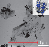 There are already several technologies that potentially allow mass production of graphene sheets--by chemical vapor deposition growth; by epitaxial growth of graphene on top of a metal surface; and various wet chemical processes of processing graphene in solution by exfoliating graphite. In new work, Englert and a group of scientists from the University Erlangen-Nuremberg, led by Andreas Hirsch, have now demonstrated the first bulk wet chemical exfoliation of graphite in association with an in situ covalent functionalization of intermediately generated graphene. With this novel chemical method, it is now possible to achieve covalently bonded functionalities without mechanical or sonochemical treatment. The covalent functionalization also protects the single-layer graphene from reaggregation and substrate-induced doping. More.... There are already several technologies that potentially allow mass production of graphene sheets--by chemical vapor deposition growth; by epitaxial growth of graphene on top of a metal surface; and various wet chemical processes of processing graphene in solution by exfoliating graphite. In new work, Englert and a group of scientists from the University Erlangen-Nuremberg, led by Andreas Hirsch, have now demonstrated the first bulk wet chemical exfoliation of graphite in association with an in situ covalent functionalization of intermediately generated graphene. With this novel chemical method, it is now possible to achieve covalently bonded functionalities without mechanical or sonochemical treatment. The covalent functionalization also protects the single-layer graphene from reaggregation and substrate-induced doping. More....
Fabrication of Nanoscale Plasmonic Sensing Structures Over Large Areas
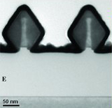 Plasmonic sensors provide a means of detecting chemical and biological species through the observation of spectral features by measurement techniques such as surface enhanced Raman spectroscopy (SERS) or surface plasmon resonance (SPR). Plasmonically active SERS substrates, such as metallic gratings or periodic metal nanowire arrays, have sub-wavelength features that enable direct coupling of normally incident electromagnetic (EM) radiation to surface plasmons. The high detection sensitivity of these methods is facilitated by EM field enhancements in the vicinity of the metallic nanostructures. Field enhancements can be achieved by controlling the spacing between nanostructures as well as the features along the length of individual nanostructures. In order to develop a full-scale plasmonic sensor, periodic nanostructures must be replicated over large-area surfaces, such as six-inch silicon wafers. By incorporating hybrid top-down and bottom-up synthesis, a versatile approach has been demonstrated for fabricating large-area plasmonic sensors. The ability to fine tune nanostructure features over large areas renders this technique highly adaptable, thereby opening up new opportunities for plasmonic sensor applications. More.... Plasmonic sensors provide a means of detecting chemical and biological species through the observation of spectral features by measurement techniques such as surface enhanced Raman spectroscopy (SERS) or surface plasmon resonance (SPR). Plasmonically active SERS substrates, such as metallic gratings or periodic metal nanowire arrays, have sub-wavelength features that enable direct coupling of normally incident electromagnetic (EM) radiation to surface plasmons. The high detection sensitivity of these methods is facilitated by EM field enhancements in the vicinity of the metallic nanostructures. Field enhancements can be achieved by controlling the spacing between nanostructures as well as the features along the length of individual nanostructures. In order to develop a full-scale plasmonic sensor, periodic nanostructures must be replicated over large-area surfaces, such as six-inch silicon wafers. By incorporating hybrid top-down and bottom-up synthesis, a versatile approach has been demonstrated for fabricating large-area plasmonic sensors. The ability to fine tune nanostructure features over large areas renders this technique highly adaptable, thereby opening up new opportunities for plasmonic sensor applications. More....
NanoBusiness NYC Conference, April 6-7 Agenda
 The NanoBusiness Commercialization Association has announced their updated program for the 2nd Annual NanoBusiness NYC Conference, which will be held will be held April 6 & 7 at the Marriott Marquis Times Square in New York City. The theme of the 2011 Conference is The Next Decade of Nanotechnology. The NYC Event brings together New York's investment community to analyze the commercialization of nanotechnology products. The event includes both keynote presentations and panel discussions. More.... The NanoBusiness Commercialization Association has announced their updated program for the 2nd Annual NanoBusiness NYC Conference, which will be held will be held April 6 & 7 at the Marriott Marquis Times Square in New York City. The theme of the 2011 Conference is The Next Decade of Nanotechnology. The NYC Event brings together New York's investment community to analyze the commercialization of nanotechnology products. The event includes both keynote presentations and panel discussions. More....
Read more on  |
Advertisement

Upcoming Events
April 5 - 6, 2011
Nanomanufacturing Micromanufacturing Conference & Exhibits
April 6 - 7, 2011
2011 NanoBusiness NYC Conference
April 9 - 11, 2011
ICMSE 2011
April 14, 2011
Nanomaterials for Biological Applications
April 24 - 29, 2011
Graphene Week
April 25 - 29, 2011
MRS Spring Meeting 2011
View Full Calendar
Upcoming Calls
NANOARCH'11
Submission Deadline April 10
Greener Nano 2011
Poster Abstracts still being accepted
AVS 58th International Symposium and Exhibition
Submission Deadline May 4
View All Calls
Advertisement

Recently Published
From Our Affiliates
Photoinduced Ordering of Block Copolymers
Nano Letters 11(3):1153-1160
Gelation behavior of polysaccharide-based interpenetrating polymer network (IPN) hydrogels
Rheologica Acta50(1):39-52
Effect of Processing Parameters on the Electrophoretic Deposition of Carbon Black Nanoparticles in Moderately Viscous Systems
Langmuir 27(6):3166-3173
Design, Fabrication, and Characterization of Three-Dimensional Single-Walled Carbon Nanotube Assembly and Applications As Thermal Sensors
IEEE Transactions on Nanotechnology 10(1):13-20
Biofunctionalized nanoneedles for the direct and site-selective delivery of probes into living cells
Biochimica Et Biophysica Acta-General Subjects 1810(3) Sp. Iss.:330-338
Advertisement

Affiliated Centers


 |
 Volume
4 Issue 3 - March 2011
Volume
4 Issue 3 - March 2011