|
The NNN Newsletter
Three Dimensional Transistor Design Maintains Moore's Law for Foreseeable Future
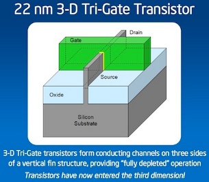 Adhering to Moore's Law of scaling of semiconductor devices and integrated circuits (ICs), the doubling of transistor packing density every eighteen months has lately become quite challenging for semiconductor manufacturers who need to address hard limits in lithographic feature resolution, increasing power dissipation per unit volume, and power utilization for mobile computing applications. As a result, new process and materials approaches are being included in semiconductor roadmaps in order to maintain this important trend, including the combination of top down and bottom up nanomanufacturing process steps, and lithographic approaches having ever-decreasing feature size and resolution. While some predictions of process approaches have included revolutionary methods incorporating bio-inspired nanostructures and processes to achieve templates with nanometer-scale critical features, it remains practical for the integrated circuit industry to maintain the process and tool infrastructure presently utilized. Therefore, acceptance of new methods and materials depends on a certain level of compatibility with existing fabrication lines. As such, the industry has been awaiting a major breakthrough that would propel technologies into the next millennium of advanced electronics and consumer products. More... Adhering to Moore's Law of scaling of semiconductor devices and integrated circuits (ICs), the doubling of transistor packing density every eighteen months has lately become quite challenging for semiconductor manufacturers who need to address hard limits in lithographic feature resolution, increasing power dissipation per unit volume, and power utilization for mobile computing applications. As a result, new process and materials approaches are being included in semiconductor roadmaps in order to maintain this important trend, including the combination of top down and bottom up nanomanufacturing process steps, and lithographic approaches having ever-decreasing feature size and resolution. While some predictions of process approaches have included revolutionary methods incorporating bio-inspired nanostructures and processes to achieve templates with nanometer-scale critical features, it remains practical for the integrated circuit industry to maintain the process and tool infrastructure presently utilized. Therefore, acceptance of new methods and materials depends on a certain level of compatibility with existing fabrication lines. As such, the industry has been awaiting a major breakthrough that would propel technologies into the next millennium of advanced electronics and consumer products. More...
Regards,
Jeff Morse, Managing Director,
National Nanomanufacturing Network
Learn More about the 
Enhanced Performance in Graphene Transistors via Interface Engineering
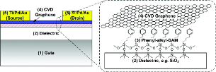 As interest has grown in electronic devices and circuits fabricated from graphene thin films due to the large intrinsic carrier mobility, a key challenge remains to establish device integration strategies that enable field effect transistors (FETs) to have mobility approaching the intrinsic value. With thin film approaches to form graphene using chemical vapor deposition (CVD) on copper foils and subsequent transfer to silicon or other substrates for final integration, graphene has become a prime candidate for a range of applications in very large scale integrated (VLSI) circuits. Recently Liu et. al. have investigated the physics associated with the dielectric-graphene interface for integrated back gated FETs by controlling some of the detrimental scattering effects via application of self-assembled monolayers (SAM). Liu et. al. present a facile approach to improve the performance of scalable graphene transistors utilizing interfacial. The results provide valuable insights into the interfacial physics of graphene FETs. These results ultimately improve the potential application of graphene transistors towards VLSI circuits and applications.
More.... As interest has grown in electronic devices and circuits fabricated from graphene thin films due to the large intrinsic carrier mobility, a key challenge remains to establish device integration strategies that enable field effect transistors (FETs) to have mobility approaching the intrinsic value. With thin film approaches to form graphene using chemical vapor deposition (CVD) on copper foils and subsequent transfer to silicon or other substrates for final integration, graphene has become a prime candidate for a range of applications in very large scale integrated (VLSI) circuits. Recently Liu et. al. have investigated the physics associated with the dielectric-graphene interface for integrated back gated FETs by controlling some of the detrimental scattering effects via application of self-assembled monolayers (SAM). Liu et. al. present a facile approach to improve the performance of scalable graphene transistors utilizing interfacial. The results provide valuable insights into the interfacial physics of graphene FETs. These results ultimately improve the potential application of graphene transistors towards VLSI circuits and applications.
More....
Swiss Researchers Boost Efficiency of Flexible Solar Cells to New World Record
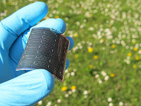 Scientists at Empa, the Swiss Federal Laboratories for Materials Science and Technology, have further boosted the energy conversion efficiency of flexible solar cells made of copper indium gallium (di)selenide (also known as CIGS) to a new world record of 18.7% - a significant improvement over the previous record of 17.6% achieved by the same team in June 2010. The measurements have been independently certified by the Fraunhofer Institute for Solar Energy Systems in Freiburg, Germany. More.... Scientists at Empa, the Swiss Federal Laboratories for Materials Science and Technology, have further boosted the energy conversion efficiency of flexible solar cells made of copper indium gallium (di)selenide (also known as CIGS) to a new world record of 18.7% - a significant improvement over the previous record of 17.6% achieved by the same team in June 2010. The measurements have been independently certified by the Fraunhofer Institute for Solar Energy Systems in Freiburg, Germany. More....
NanoBusiness Interview -
Dr. J. Steven Rutt, Partner & Chairman, Nano Team, Foley & Lardner
 In this month's interview, we talk to Dr. J. Steven Rutt, Partner and Chairman of the Nanotechnology Industry Team at Foley & Lardner LLP. Dr Rutt's practice includes patent counseling, patent prosecution, IP licensing and agreements, including technology transfer carried out under the Bayh-Dole Act, patent landscaping and clearance opinions, due diligence, patent litigation support, trade secrets, and trademarks. Dr. Rutt is a frequent writer and conference presenter with respect to nanotechnology and the law, actively helping to lead and participate in Foley's Nanotechnology Industry Team. Currently, he is editor of the blog, www.nanocleantechblog.com. He is also the author of a dozen scientific publications and inventor on four patents. His experience includes nine years of hands-on research in polymer synthesis and morphological studies, and his experience in private industry includes two years of corporate chemical research with NTT in Tokyo, Japan. Dr. Rutt's legal papers have been published widely, including publications such as Nanotechnology Law and Business Journal, Journal of the Patent & Trademark Office Society, The SciTech Lawyer, and the Legal Times. More.... In this month's interview, we talk to Dr. J. Steven Rutt, Partner and Chairman of the Nanotechnology Industry Team at Foley & Lardner LLP. Dr Rutt's practice includes patent counseling, patent prosecution, IP licensing and agreements, including technology transfer carried out under the Bayh-Dole Act, patent landscaping and clearance opinions, due diligence, patent litigation support, trade secrets, and trademarks. Dr. Rutt is a frequent writer and conference presenter with respect to nanotechnology and the law, actively helping to lead and participate in Foley's Nanotechnology Industry Team. Currently, he is editor of the blog, www.nanocleantechblog.com. He is also the author of a dozen scientific publications and inventor on four patents. His experience includes nine years of hands-on research in polymer synthesis and morphological studies, and his experience in private industry includes two years of corporate chemical research with NTT in Tokyo, Japan. Dr. Rutt's legal papers have been published widely, including publications such as Nanotechnology Law and Business Journal, Journal of the Patent & Trademark Office Society, The SciTech Lawyer, and the Legal Times. More....
Read more on  |


Advertisements


Upcoming Events
May 30 - June 1, 2011
EuroNanoForum 2011 Budapest
May 31 - June 3, 2011
The 55th International Conference on Electron, Ion, and Photon Beam Technology and Fabrication
June 1 - 3, 2011
Sustainable Remediation 2011
June 5 - 7, 2011
SME Annual Conference: Manufacturing Velocity
June 6 - 8, 2011
TAPPI 2011 International Conference on Nanotechnology for Renewable Materials
June 7 - 9, 2011
Nanotech China 2011 - Shanghai
View Full Calendar
Upcoming Calls
6th Intl Congress of Nano Bio Clean Tech
Submissions until June 15
Nanomanufacturing Summit 2011
Submissions accepted until July 15
2011 MRS Fall Meeting
Submissions accepted until June 21
View All Calls
Advertisement

Recently Published
From Our Affiliates
Nanoparticle-Driven Assembly of Block Copolymers: A Simple Route to Ordered Hybrid Materials
J. Am. Chem. Soc. 133(17):65136516
Predicting the Effect of the Homogenization Pressure on Emulsion Drop-Size Distributions
Ind. Eng. Chem. Res. 50(10):6089-6100
Hybrid Integration of Photonic Crystal Membrane Lasers via Postprocess Bonding
Photonics Journal, IEEE, 3(3):375-380
Using the Fact that Wetting Is Contact Line Dependent
Langmuir, 27(7):3693-3697
Synthetic Mimics of Antimicrobial Peptides from Triaryl Scaffolds
J. Med. Chem. 54(7):2241-2254
Affiliated Centers


|
 Volume
4 Issue 5 - May 2011
Volume
4 Issue 5 - May 2011