| Email not displaying correctly? View it in your browser. |
 Volume
5 Issue 3 - March 2012
Volume
5 Issue 3 - March 2012 |
|
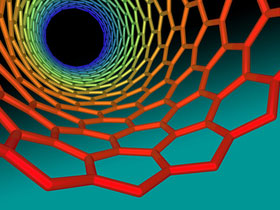
Assessing the Economic Impact of Nanotechnology: The Role of Nanomanufacturing
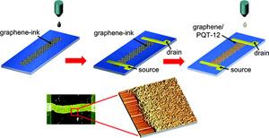
In developing a strategy for the National Nanotechnology Initiative (NNI), the President's Council of Advisors on Science and Technology (PCAST) have emphasized the need to enable more effective technology transfer and provide added focus on nanomanufacturing and commercialization. These objectives are intended to foster needed economic development within the U.S., while also providing a return on investment (ROI) for the federal government's long-term support of the NNI. While various interpretations can be made from the PCAST reports' (NNI report, Advanced Manufacturing Report) recommendations, one thing is very clear: the linkage between nanomanufacturing and commercialization. While the NNI's investment has had a significant impact on our understanding of nanoscience, and has established the U.S. as the global leader in nanotechnology, nanomanufacturing represents the vehicle by which the innovations of the nanosciences will transition the valley of death towards new and enhanced consumer products. Regards, Learn More about the Inkjet-Printed Graphene Flexible Electronics
Calculating the Cost of Advanced Manufacturing
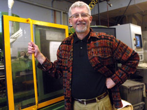
For Tim Gutowski, advanced manufacturing is an opportunity not just to boost employment, but also to improve the environment. The Environmentally Benign Manufacturing group studies the life cycle of new technologies. Gutowski heads MIT's Environmentally Benign Manufacturing research group, which looks at the environmental costs and impacts associated with manufacturing traditional materials such as concrete and steel, as well as advanced and emerging technologies such as semiconductors, photovoltaics, and nanomaterials such as carbon nanotubes. National Nanotechnology Coordination Office Welcomes New Director
The National Nanotechnology Coordination Office (NNCO) is pleased to announce the appointment of Dr. Robert Pohanka as the Director of the NNCO. Dr. Pohanka joins the NNCO after serving as the Director of the Defense Venture Catalyst Initiative (DeVenCI), where he led and directed the strategy for finding private sector technologies, developed independently of DoD, and transitioned them to DoD Research, Development and Acquisition. "We are very pleased that Dr. Pohanka will be joining our team here at the NNCO," said Dr. Sally Tinkle, Deputy Director of the NNCO and EHS Research Coordinator. "Dr. Pohanka's proven success in technology transfer and commercialization will serve the NNI well and better position the NNI to capitalize on the tremendous promise of nanotechnology." |
Advertisements
Job Opportunities Post Baccalaureate Fellow Executive Director, Office for Research Safety Upcoming Events April 4-5, 2012 April 9-13, 2012 April 10-13, 2012 April 16-20, 2012 Upcoming Calls IEEE NANO 2012 SENN2012 - International Congress on Safety of Engineered Nanoparticles and Nanotechnologies Seeing at the Nanoscale 2012 Advertisements
Recently Published Evaporation-induced cavitation in nanofluidic channels
Probing and repairing damaged surfaces with nanoparticle-containing microcapsules
Additive-Driven Assembly of Block Copolymer-Nanoparticle Hybrid Materials for Solution Processable Floating Gate Memory
Cooperative Assembly of Hydrogen-Bonded Diblock Copolythiophene/Fullerene Blends for Photovoltaic Devices with Well-Defined Morphologies and Enhanced Stability
Adsorption and Photochemical Properties of a Molecular CO2 Reduction Catalyst in Hierarchical Mesoporous ZSM-5: An In Situ FTIR Study Affiliated Centers |
|
Subscribe / Unsubscribe from this list. Our mailing address is: The National Nanomanufacturing Network 374 Lederle Graduate Research Center 710 N. Pleasant Street University of Massachusetts Amherst, MA 01003 Our email address is: nnn@nanomanufacturing.org Our phone number is: (413) 577-0570 Copyright (C) 2012 The National Nanomanufacturing Network All rights reserved. Supported by the National Science Foundation under Grant No. CMMI-1025020. |
|