| Email not displaying correctly? View it in your browser. |
 Volume
6 Issue 1 - January 2013
Volume
6 Issue 1 - January 2013 |
|
EU's Graphene Flagship Initiative: A Public-Private Partnership of Unprecedented Scale  Graphene has been the subject of an explosion of technical research in recent years as a result of its unique combination of superior properties. It has become the starting point for disruptive technologies in a wide range of fields including high performance computing, transparent conductors, printed electronics, displays, solar photovoltaics, and sensors. Pathways to large area, high throughput production of graphene materials have been established, and key cases emerging from research labs around the globe have demonstrated the advantages of graphene for the applications noted above. The European Commission recently announced graphene as one of the EU's first 10-year, 1 Billion euro Future $amp; Emerging Technology (FET) flagships. The goal of the Graphene Flagship is to accelerate the path of graphene and related layered materials from academic laboratory research to scaled commercialization. The resulting societal benefit and subsequent revolutionizing of multiple industry sectors should create substantial economic growth and new jobs in the EU. The recent announcement is noteworthy as it is launching a coordinated public-private partnership research initiative of unprecedented scale. Regards, Learn More about the DNA and Quantum Dots: All That Glitters is Not Gold
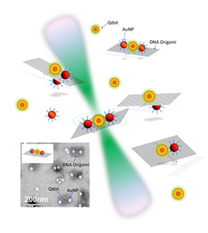
A team of researchers at the National Institute of Standards and Technology (NIST) has shown that by bringing gold nanoparticles close to the dots and using a DNA template to control the distances, the intensity of a quantum dot's fluorescence can be predictably increased or decreased.* This breakthrough opens a potential path to using quantum dots as a component in better photodetectors, chemical sensors and nanoscale lasers. Anyone who has tried to tune a radio knows that moving their hands toward or away from the antenna can improve or ruin the reception. Although the reasons are well understood, controlling this strange effect is difficult, even with hundred-year-old radio technology. Similarly, nanotechnology researchers have been frustrated trying to control the light emitted from quantum dots, which brighten or dim with the proximity of other particles. The State of Nanoimprinted Polymer Organic Solar Cell Technology
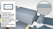
Many researchers are investigating the development of flexible solar cells in hopes of improving efficiency and lowering manufacturing costs. As an important member of the organic photovoltaics (OPV) family, polymer solar cells draw the most research interest, due to the relatively high power conversion efficiency achieved. However, compared to the high efficiencies (>10%) of inorganic solar cells, the best polymer solar cells (6-7%) still show a lower efficiency. Flexible Organic Photovoltaic Cells with In-situ Non-thermal Photoreduction of Spin Coated Graphene Oxide Electrodes
|
Advertisements
Job Opportunities Cleanroom Laboratory Manager Assistant Professor, School of Mechanical, Industrial, and Manufacturing Engineering Photolithography Engineer Upcoming Events February 22, 2013 February 24-28, 2013 March 25-28, 2013 Featured Video
Advertisements
Recently Published Direct Patterning of Engineered Ionic Gold Nanoparticles via Nanoimprint Lithography
Functional Protein Microarrays by Electrohydrodynamic Jet Printing
Colorimetric Protein Sensing Using Catalytically Amplified Sensor Arrays
Addition of perfluorocarbons to alginate hydrogels significantly impacts molecular transport and fracture stress
Development of antimicrobial stainless steel via surface modification with N-halamines: Characterization of surface chemistry and N-halamine chlorination
Affiliated Centers |
|
Subscribe / Unsubscribe from this list. Our mailing address is: The National Nanomanufacturing Network 374 Lederle Graduate Research Center 710 N. Pleasant Street University of Massachusetts Amherst, MA 01003 Our email address is: nnn@nanomanufacturing.org Our phone number is: (413) 577-0570 Copyright (C) 2013 The National Nanomanufacturing Network All rights reserved. Supported by the National Science Foundation under Grant No. CMMI-1025020. |
|
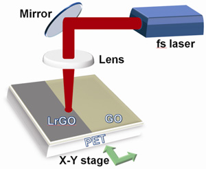 Researchers from Greece demonstrated a groundbreaking methodology for controlled in-situ reduction of spin-casted graphene oxide (GO) nanometric films on flexible substrates and the subsequent realization of highly conductive and transparent electrodes for flexible organic photovoltaics (OPV). This technique is the first reported to be compatible with temperature sensitive substrates in the sense that it achieves reduction of films on flexible substrates in a single step, in contrast to the approaches utilized so far. Furthermore the featured work provides a new insight in the relevant scientific community considering that it is experimentally clarified that efficient photoreduction of GO can be achieved by exploiting non-thermal processes occurring upon ultrafast laser treatment. This suggests that there is no need for high temperature treatments that potentially destroy the integrity of the graphene lattice as well as the flexibility of the underlying substrate.