| Email not displaying correctly? View it in your browser. |
 Volume
6 Issue 3 - March 2013
Volume
6 Issue 3 - March 2013 |
|
Nanomanufacturing Accelerates Body-Worn Electronic Monitoring Systems 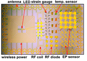 As we continue to promote the economic and societal benefits of nanotechnology, advanced nanomanufacturing techniques are paving the road towards more integrated systems with increased functionality, scaled production platforms, and lower cost that will impact a broad range of industries. Nanomanufacturing has arguably had the largest impact in the area of flexible electronics and systems, affecting a range of product applications including displays, photovoltaics, lighting, energy storage, and printed electronics circuits. Perhaps the area of highest impact could be that in the area of devices interacting with the human body to extract specific biometrics for various purposes such as point-of-care health diagnostics, therapeutic treatment, or general activity monitoring. While these concepts have been around for decades, the key factors of technology push and market pull are now beginning to align in a manner that will accelerate and sustain the translational R&D necessary for these applications to grow. From a market pull perspective, the increasing cost of hospital and medical care combined with the growth of an aging population will necessitate in-home monitoring and out-patient care. Nanotechnology will most certainly provide the market push to meet these challenges. Regards, Learn More about the Commercializing Graphene and Other Novel 2D Structures
Lux Research recently published a report entitled "Is Graphene the Next Silicon…Or Just the Next Carbon Nanotube?". Apart from eliciting a wince reaction from those of us who have worked and are working with carbon nanotubes (CNTs), the title asks a very valid question that begs an answer - how can we do a better job with graphene than we did with CNTs? 3Qs: The 3D Printing of Tomorrow
Ahmed Busnaina, the William Lincoln Smith Professor and director of the NSF Nanoscale Science and Engineering Center for High-rate Nanomanufacturing at Northeastern, has developed a method called directed assembly that he calls the 3-D printing of tomorrow. It is faster, cheaper, and more versatile than traditional 3-D printing, and he said it could enable a wave of innovation not currently feasible. news@Northeastern asked Busnaina to describe this process and its potential impact in areas such as health, electronics, and the environment. 'Metasurfaces' to Usher in New Optical Technologies
The metasurfaces could make possible "planar photonics" devices and optical switches small enough to be integrated into computer chips for information processing and telecommunications, said Alexander Kildishev, associate research professor of electrical and computer engineering at Purdue University. |
Advertisements
Job Opportunities Postdoctoral Appointee - Nanotechnology Principal Scientist / Sr. Principal Scientist, Nanotechnology Nanosystems Engineer/Physical Scientist Upcoming Events March 30 - April 7, 2013 April 9-10, 2013 April 26, 2013 Featured Video
Advertisements
Recently Published Graphene-Supported Pt, Ir, and Pt-Ir Nanoparticles as Electrocatalysts for the Oxidation of Ammonia
Effect of Al2O3 nanoparticles on bacterial membrane amphiphilic biomolecules
Directed assembly of conducting polymers on sub-micron templates by electrical fields
Temperature dependence of serum protein adsorption in PEGylated PNIPAm microgels
Affiliated Centers |
|
Subscribe / Unsubscribe from this list. Our mailing address is: The National Nanomanufacturing Network 374 Lederle Graduate Research Center 710 N. Pleasant Street University of Massachusetts Amherst, MA 01003 Our email address is: nnn@nanomanufacturing.org Our phone number is: (413) 577-0570 Copyright (C) 2013 The National Nanomanufacturing Network All rights reserved. Supported by the National Science Foundation under Grant No. CMMI-1025020. |
|
 Graphene has been a really hot topic since its discovery in 2004 when atomically thin sheets of carbon were peeled off graphite by University of Manchester scientists Andre Geim and Konstantin Novoselov. Since then, the material has received great publicity, significant funding and more than a little hype in the media. So how do we assess the potential of graphene and its increasing number of compounds and planar relatives?
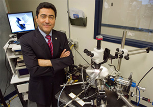
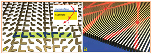 New optical technologies using "metasurfaces" capable of the ultra-efficient control of light are nearing commercialization, with potential applications including advanced solar cells, computers, telecommunications, sensors and microscopes.