Email not displaying correctly? View it in your browser. | |||||||||||
 | |||||||||||
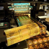 Continuous Roll-Process Technology for Transferring and Packaging Flexible LSIA research team led by Professor Keon Jae Lee from the Korea Advanced Institute of Science and Technology (KAIST) and by Dr. Jae-Hyun Kim from the Korea Institute of Machinery and Materials (KIMM) has jointly developed a continuous roll-processing technology that transfers and packages flexible large-scale integrated circuits (LSI), the key element in constructing the computer's brain such as CPU, on plastics to realize flexible electronics (Advanced Materials, "Simultaneous Roll Transfer and Interconnection of Flexible Silicon NAND Flash Memory"). Professor Lee previously demonstrated the silicon-based flexible LSIs using 0.18 CMOS (complementary metal-oxide semiconductor) process in 2013 (ACS Nano, "In Vivo Silicon-based Flexible Radio Frequency Integrated Circuits Monolithically Encapsulated with Biocompatible Liquid Crystal Polymers") and presented the work in an invited talk of 2015 International Electron Device Meeting (IEDM), the world's premier semiconductor forum. Highly productive roll-processing is considered a core technology for accelerating the commercialization of wearable computers using flexible LSI. However, realizing it has been a difficult challenge not only from the roll-based manufacturing perspective but also for creating roll-based packaging for the interconnection of flexible LSI with flexible displays, batteries, and other peripheral devices. To overcome these challenges, the research team started fabricating NAND flash memories on a silicon wafer using conventional semiconductor processes, and then removed a sacrificial wafer leaving a top hundreds-nanometer-thick circuit layer. Next, they simultaneously transferred and interconnected the ultrathin device on a flexible substrate through the continuous roll-packaging technology using anisotropic conductive film (ACF). The final silicon-based flexible NAND memory successfully demonstrated stable memory operations and interconnections even under severe bending conditions. This roll-based flexible LSI technology can be potentially utilized to produce flexible application processors (AP), high-density memories, and high-speed communication devices for mass manufacture. Professor Lee said, "Highly productive roll-process was successfully applied to flexible LSIs to continuously transfer and interconnect them onto plastics. For example, we have confirmed the reliable operation of our flexible NAND memory at the circuit level by programming and reading letters in ASCII codes. Out results may open up new opportunities to integrate silicon-based flexible LSIs on plastics with the ACF packing for roll-based manufacturing." Dr. Kim added, "We employed the roll-to-plate ACF packaging, which showed outstanding bonding capability for continuous roll-based transfer and excellent flexibility of interconnecting core and peripheral devices. This can be a key process to the new era of flexible computers combining the already developed flexible displays and batteries." |
|||||||||||
 New Center on Nano-safety Research at T.H. Chan Harvard School of Public HealthNational Institutes of Health (NIH) and its National Institute of Environmental Health Sciences (NIEHS) just announced the funding of a new interdisciplinary Nano-safety Center at the T. H. Chan Harvard School of Public Health.  Electronic Circuits Printed
|
August 2016
|
||||||||||
| |||||||||||