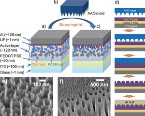
| Lee et. al demonstrate a simple, low-cost method to imprint nanoscale patterns in the surface of polymer-based photovoltaic materials systems for enhanced power conversion efficiency. |
Reviewed by Jeff Morse, Ph.D, National Nanomanufacturing Network
While polymer-based photovoltaic cells represent a key competitive approach toward economically affordable photovoltaic cells, the challenge remains to enhance the power conversion efficiency for these materials systems. Performance optimization is difficult as photon absorptions, carrier transport, and carrier collection properties must be considered.
One of the more popular organic photovoltaic material systems consists of blends of polythiophene derivatives and fullerenes making up a single bulk heterojunction active layer. Interconnected domains are formed as the components phase-segregate to form the heterojunction interface. Since these domains are highly disordered, many are isolated preventing the associated charge carriers from being collected. Additionally, excitons generated by incident photons have typical diffusion lengths on the order of 10 nm for polymer-based photovoltaics, therefore the active layer design must be of similar dimension.

Lee et.al. demonstrate the use anodic alumium oxide (AAO) molds as a means to generate nanoscale surface morphology on polymer-based bulk heterojunction materials. An AAO membrane with pore diameter on the order of 100 nm is used to template nanoscale patterns in the surface of a poly(3-hexylthiophene) (P3HT)/(6,6)-phenyl-C61-butyric acid methyl ester (PCBM) active layer.. Interpenetrating nanoelectrodes are subsequently formed by evaporating a LiF/Al film on the textured P3HT/PCBM layer.
The authors tested the nanoimprinted cells, comparing their performance to planar cell design both before and after thermal annealing. Results show a 25% increase for thermally annealed, nanoimprinted cell designs, demonstrating power conversion efficiency of 4.43%. These results are attributed a combination of parameters—the number of absorbed photons, the number of carriers generated by charge separation at the heterojunction interface, and the charge-collection efficiency. The nanoimprinted interpenetrating electrode would benefit each of these parameters. Furthermore, it is speculated that the thermal annealing steps improved the heterojunction domain properties by improving the crystallinity of the domain.
In summary, a simple, low-cost method to imprint nanoscale patterns in the surface of polymer-based photovoltaic materials systems has been described. Further improvements may be expected as the patterns are scaled to smaller, denser, higher aspect ratio dimensions.
Image from Lee JH, Kim DW, Jang H, Choi JK, Geng J, Jung JW, Yoon SC, and Jung H-T. 2009. Enhanced Solar Cell Efficiency in bulk-heterojunction Polymer Systems Obtained by Nanoimprinting with Commercially Available AAO Membrane Filters. Small 22 Jun. 5pp. DOI: 10.1002/smll.200900666.Copyright Wiley-VCH Verlag GmbH & Co. KGaA. Reproduced with permission.
This work is licensed under a Creative Commons Attribution-NonCommercial-NoDerivs 3.0 Unported.
