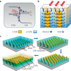
| In three new studies, the ability to design 3D materials architectures provides a versatile approach towards optimization of device properties for enhanced performance in product applications. |
Reviewed by Jeff Morse, Ph.D, National Nanomanufacturing Network
- Fan Z, et al. 2009. Three-dimensional Nanopillar-array Photovoltaics on Low-cost and Flexible Substrates. Nature Materials 8: 648-653. DOI: 10.1038/NMAT2493.
- Haberkorn N, et al. 2009. Template-assisted Fabrication of Free-standing Nanorod Arrays of a Hole-Conducting Cross-Linked Triphenylamine Derivative: Toward Ordered Bulk-heterojunction Solar Cells. ACS Nano 3(6): 1415-1422. DOI: 10.1021/nn900207a.
- Cheah SK, et al. 2009. Self-supported Three-dimensional Nanoelectrodes for Microbattery Applications. Nano Letters 9(9): 3230-3233. DOI: 10.1021/nl9014843.
While it has been known for many years that three-dimensional (3D) nanoscale architectures enhance the performance of energy storage and power generating devices, it has not been until recently that the tools to fabricate such structures are readily available for scalable processes. High surface area materials have previously demonstrated performance benefits for electrodes and catalyst supports in battery and fuel cell technologies, but new fabrication and integrated process capabilities now make it possible to address specific limitations of a given technology by enabling 3D designs.
For example, Li-ion batteries must balance electrode resistance, lithium uptake and capacity, ion transport, and cycling stability. Similarly, photovoltaic cells must balance photon absorption lengths, carrier or exciton transport properties, carrier collection efficiency, and electrode properties in order to optimize cell performance. For fuel cells, electrodes require an intricate reaction interface balancing electron and ion transport while providing adequate reactant diffusion and accessibility. In all of these cases, the ability to design 3D materials architectures provides a versatile approach towards optimization of these and other device properties for the resulting applications.

In a similar approach to organic solar cells, Haberkorn et. al. investigate the use of AAO templates to create nanopillars of hole conducting polymers. Here, the authors describe the final structure as a well-defined photoactive layer consisting of nanorods embedded within an electron-conducting matrix. In order to fabricate the structure, the polymer nanorods must demonstrate mechanical stability before the subsequent electron-conducting polymer coating is spin-coated over the array. To form an AAO template with pores approximately 100 nm diameter and 1 µm thick, the authors combine a solution wetting process with a thermal imprinting step in order to completely fill the pores and create mechanically stable nanorods with good adhesion to the substrate. The AAO template is spin-cast with a cross-linkable divinyltriphenylamine (DVTPA) hole-conducting polymer and dried. Then an ITO/glass cover slide is pressed on top of the AAO template. The ITO/glass surface is prefunctionalized with vinyltrimethoxysilane in order to provide enhanced adhesion of the DVPTA to the ITO. After clamping the ITO/glass to the AAO template, a thermal cure in vacuum is conducted at 150°C for 180 min, sufficiently above the DVPTA melting point to reflow the polymer resulting in uniform, solid nanorod arrays. The aluminum substrate and AAO templates are selectively removed by wet chemical etching from the backside, resulting in mechanically stable hole-conducting polymer nanorods.
Similarly for Li-ion battery structures, Cheah et. al. utilize AAO templates to form high surface area Aluminum nanorods by pulsed electrodeposition. The AAO template is then selectively removed resulting in an array of Al nanorods having diameter of approximately 200 nm, with typical spacing’s of 40 nm. Using atomic layer deposition (ALD), the authorsuniformly coat the high aspect ratio (10:1) nanorods with a 17 nm layer of titanium oxide. ALD proved critical in fully coating the nanorod arrays in a one-step process. Test results demonstrate that the 3D architecture exhibited greater than one order of magnitude charge storage capacity as compared to a 2D structure with the same footprint.
In each of the examples discussed above, the merits of 3D integration for power and energy storage devices has been demonstrated. Additional templating approaches, such as self assembly by block copolymers or nanoimprint lithography, may further improve the scale of the nanostructures, as well as the integration compatibility. The key factor is that process and tools suitable to optimize these devices and materials for a given application has now reached the point where the path to scaled production is more favorable. As such, it may be anticipated that more of these structures will impact commercial markets in the near future.
Image reprinted by permission from Macmillan Publishers Ltd: Nature Materials, advance online publication, 5 July 2009 (DOI: 10.1038/nmat2493).
