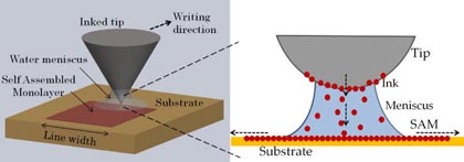
| Dip pen nanolithography (DPN) has emerged as a versatile nanofabrication tool enabling the synthesis of nanoscale features via mass or energy transfer from an atomically sharp, inked tip to a substrate surface. Recently, Saha and Culpepper utilized DPN as a case study to evaluate and characterize key tip-based processes for nanomanufacturing, and subsequently how the process characterization can be used to identify the necessary control and system design parameters to achieve high throughput, high quality nanomanufacturing. This article presents an effective analysis of DPN nanomanufacturing process parameters which provides assessment of process limitations and considerations to be made prior to embarking a process scale-up. Such analysis enables critical assessment of the commercial viability of this emerging nanomanufacturing tool prior to investment for the production of value-added, nano-enabled technologies. |
Reviewed by Jeff Morse, PhD, National Nanomanufacturing Network
- Sourabh SK and Culpepper ML. 2011. Characterization of the dip pen nanolithography process for nanomanufacturing. Journal of Manufacturing Science and Engineering. 133(4), 041005. http://dx.doi.org/10.1115/1.4004406
Dip pen nanolithography (DPN) has emerged as a versatile nanofabrication tool enabling the synthesis of nanoscale features via mass or energy transfer from an atomically sharp, inked tip to a substrate surface. Such tip-based processes facilitated by instruments such as atomic force or scanning tunneling microscope platforms have broad applications in biomedical diagnostics, sensors, combinatorial chemistry, and electronics. At present, most implementations of tip-based nanofabrication processes and systems exist within research environments conducting fundamental studies or limited prototyping of value added products and devices. In order to transcend the gap from research laboratory to full-scale manufacturing for these applications, high throughput, high quality, repeatable fabrication of nanoscale features is required. Presently, DPN process scale-up is limited due to a lack of process understanding and models, and manufacturing equipment platforms enabling the necessary closed loop process control.

With the goal of establishing a DPN process model having the ability to predict process performance, quantify the practical process limits in terms of feasible rates and quality, and correlate process capability to process and system parameters, the authors characterized the scaled manufacturing capability of DPN processes considering a variety of process parameters and outcomes. These process parameters included processing rate or writing speed, tool life, and feature quality, which were further augmented by control of process parameters such as temperature, humidity, ink properties, and tool functionality. In order to establish the control relationship between various parameters, as well as quantify key process limitations, a sensitivity analysis was additionally conducted. From the process characterization and sensitivity analysis a predictive capability was demonstrated that could be utilized to identify the manufacturability of specific nanotechnology-enabled products through an improved understanding of the necessary economy of scale that must be achieved. An interesting outcome of this study was the conclusion of process niches where DPN could be exploited. From the analysis it was found that process control was significantly less stringent at high writing speeds with smaller features. As such, applications where these conditions are needed could take advantage of less complex, smaller and more affordable systems for manufacturing scale-up. Furthermore, while the process characterization was limited to existing DPN system designs and capabilities, the analysis provided insights into potential future system design implementations that could enhance DPN manufacturability. Examples of new system implementations that would enhance throughput and rate include forced-ink flow and parallelization. Improved fixturing could enable rapid tool change during high quality line writing. Further development and refinement of DPN process models will include environmental conditions, tip geometrical factors impacting the meniscus properties, and properties of the ink molecules utilized.
In summary, an effective analysis of DPN nanomanufacturing process parameters has been conducted providing assessment of process limitations and considerations to be made prior to embarking a process scale-up. Such analysis enables critical assessment of the commercial viability of this emerging nanomanufacturing tool prior to investment for the production of value-added, nano-enabled technologies.
Figure reprinted with permission pending from Sourabh SK and Culpepper ML. 2011. Characterization of the dip pen nanolithography process for nanomanufacturing. Journal of Manufacturing Science and Engineering. 133(4), 041005. http://dx.doi.org/10.1115/1.4004406. Copyright 2011 American Society of Engineers.
