Skip to content Skip to navigation

Game Changing Nanomanufacturing Technology: Keeping a Cautious Eye Towards the Future

Written by: 
Jeff Morse, PhD

Assessing the impact of emerging nanomanufacturing science and research requires an objective evaluation of the road to commercialization. In many instances, the path from “lab to fab” is filled with potholes, barriers, and detours, requiring new technologies to demonstrate significant benefits in both cost and performance in order to supplant existing technology and infrastructure. A prime example includes processes and materials being considered for semiconductor integrated circuit manufacturing. While several emerging nanomanufacturing methods, such as directed self assembly (DSA), nanoimprint lithography (NIL), and atomic layer deposition (ALD) are gaining acceptance as a competitive approach for specific steps within the integration sequence, the process for industry adoption remains lengthy and expensive. As a result, the impact of nanomanufacturing methodologies on existing industries and infrastructure has been limited to date. Conversely, the utilization of nanocomposite materials has had a significant impact on numerous industries including aerospace, sporting goods, automotive, and medical devices, enabling functional materials providing higher strength, lighter weight, and lower cost for a broad range of applications. The latter is a better example of a game changing technology providing a completely new approach and infrastructure to solve industry’s problem, and further expanding markets, products, and profits.
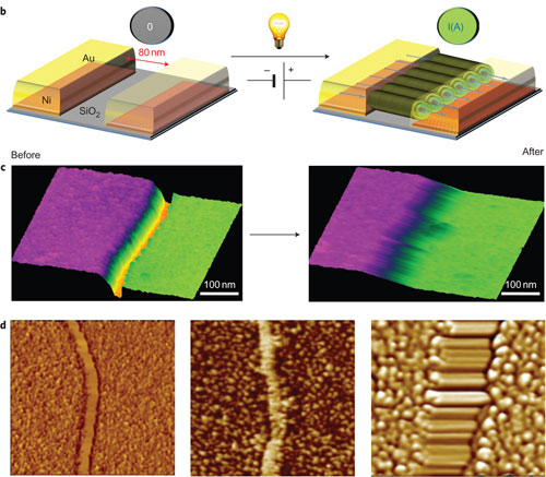
b A solution of triarylamine 1 (a, 1 mg ml1 in C2H2Cl4) is drop-cast, in the dark, on nanopatterned gold/nickel electrodes (b: trench width, 100 µm; length, 0.08 µm; ”V = 0.3–0.8 V). The device is then submitted to white light irradiation (power density, ~10 W cm2 for 10 s), which enables the production of a catalytic quantity of radicals 1•+. The triarylammonium 1•+ induces a supramolecular polymerization with neutral 1 that results in the self-assembly of STANWs aligned in the direction of the electric field and strongly connecting the two electrodes. c, Left: topography of the opened gap seen by AFM before light irradiation. Right: topography of the closed gap filled with STANWs after light irradiation. d, Left: AFM phase image of a fibre-free gap (surface scale, 1,500 x 1,500 nm2) before light irradiation. Middle: AFM phase image of a gap filled with STANWs (surface scale, 1,500 × 1,500 nm2) after light irradiation. Right: AFM zoom into the gap, which is filled with STANWs after light irradiation (surface scale, 250 × 250 nm2).
Flexible electronics represents a high growth, emerging market opportunity for commercial products such as photovoltaics, displays, energy storage, and sensors. At present, approaches to flexible electronics incorporate a semiconductor integrated circuit paradigm in which lower temperature processes and materials are incorporated to build low performance circuits and devices sufficient for the range of product applications being targeted. In this context, organic, inorganic, and hybrid materials are being investigated for semiconductor devices, conductor interconnects, and dielectric components. Key limitations of organic polymer materials for electronic applications include poor electronic transport properties, stability, and lack of adequate conductors for device/circuit integration. As a result, flexible electronics are fabricated using a combination of additive and subtractive processes, along with patterning and alignment steps. The cost-performance requirements for near term product applications are such that low-resolution lithography is sufficient to pattern devices over large areas, further utilizing vacuum deposition and etching processes. As materials and process innovations have been steadily achieved resulting in improvements in electronic device performance, organic materials performance still lags behind inorganic or hybrid materials, therefore high temperature or vacuum processes are still required. One key element of flexible electronics, however, soft interconnects having even better conductivities and limited interface resistance values with metals are needed for low-power plastic electronics, in particular for the miniaturization of devices at the nanoscale.

Recently, Faramarzi et.al., reported on the self-assembly of supramolecular organic nanowires. The interesting aspect of the reported research was the ability to both trigger the construction of the nanowires in solution through exposure to light, but also to direct the nanowire assembly between prefabricated electrode structures on a substrate using an applied electric field. The authors described their investigation of the self-assembly of organic nanowires between two metallic electrodes from a solution of triarylamine derivative, under the simultaneous action of light and electric field triggers. The resulting nanowire ensembles exhibit a combination of large conductivity values (>5x10³ S/m) and a low interface resistance (<2x10⁻⁴ Ω m) to the metal electrodes. Additionally, the resistance of nanowires in series with metal interfaces systematically decreases when the temperature is lowered to 1.5 K, revealing an intrinsic metallic behavior. The ease of solution processing, the light-triggered self-assembly and the intrinsic self-limiting supramolecular process were shown to enable the insertion of organic interconnects in pre-determined positions by means of a bottom-up approach, making possible the addressed control of nanoscale organic circuits. While game changing is a term that should be used cautiously for new technologies, the reported results, if further developed towards an integration strategy, represent a game changing technology for flexible electronic systems. And certainly could represent an extraordinarily useful tool for the next generation of smart materials. Finally, the versatile chemical structure of the organic nanowires could enable additional opportunities for tuning the electrical properties by straightforward variations using classical organic chemistry and synthesis approaches.

Reference

  • Faramarzi V, Niess F, Moulin E, Maaloum M, Dayen JF, Beaufrand B, Zanettini S, Doudin B, Giuseppone N. 2012. Light-triggered self-construction of supramolecular organic nanowires as metallic interconnects. Nature Chemistry. http://dx.doi.org/10.1038/nchem.1332 

Figure reprinted with permission from Macmillan Publishers Ltd: Faramarzi V, Niess F, Moulin E, Maaloum M, Dayen JF, Beaufrand B, Zanettini S, Doudin B, Giuseppone N. 2012. Light-triggered self-construction of supramolecular organic nanowires as metallic interconnects. Nature Chemistry. http://dx.doi.org/10.1038/nchem.1332