
Polymer solar cells (PSCs) are being actively developed for applications in which large area, high-rate solution based processes provide a low-cost alternative to more traditional photovoltaic device technologies. Progress in PSC performance has demonstrated power conversion efficiency exceeding 10% for tandem device architectures, thereby opening the door for competitive cost-performance trade-off for applications such as building integrated photovoltaics, or chargers for portable electronic devices. A related opportunity is transparent PSCs that could be used to generate power from windows on homes and buildings while still allowing people to see outside. While such a smart window technology for generating electricity could find widespread use, the cost and performance targets are even more critical in order to gain market entry. From a technology standpoint, the PSC would have to convert mainly infrared light to electricity, not the visible part of the spectrum, leaving the cells at least 70% transparent to the human eye, while demonstrating power conversion efficiency approaching that of normal PSCs. For manufacturing, the cells would have to be made through solution processing in order to achieve the necessary economy of scale for market acceptance, while further enhancing the value proposition through an extended lifecycle. All of these are significant challenges for the standard PSCs, let alone the added requirements to achieve transparency.
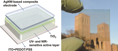
The photoactive polymer used was a specific PBDTT-DPP, PCBM blend that combines the spectral properties of each component in the blend, providing a low bandgap polymer with strong photosensitivity in the 650-850 nm wavelength range, and average transmission of 68% over the entire visible spectrum (400-650 nm), thereby ensuring effective harvesting of the UV and NIR photons while transmitting most visible photons. The authors used a commercially available transparent indium tin oxide (ITO) substrate on which the photoactive layers were cast, and utilized a composite cathode layer on top of the photoactive layer synthesized via solution processing. The transparent electrode composition included AgNWs, titania (TiO2) sol-gel, and ITO nanoparticle fillers, which when combined provide an optimal balance of visible transparency, conductivity, and efficiency through optimization of the interface between the photoactive layer and transparent conductor. Characterization of the integrated PSC devices demonstrated excellent transparency in the visible regime, with very reasonable open circuit voltages (Voc), fill-factor (FF), and power conversion efficiency in the 4-5 % range depending on which side the device was illuminated from, and whether a reflector was used on the backside. Thus, a promising materials and synthesis approach has been reported opening the window, so to speak, for a visibly transparent PSC technology. Furthermore, the demonstration of all-solution based processing compatible with existing manufacturing platforms such as ink-jet printing or roll-to-roll processing make this a serious candidate for next generation building integrated photovoltaic power systems.
Reviewed by Jeff Morse, PhD, National Nanomanufacturing Network
- Chen CC, Dou L, Zhu R, Chung CH, Song TB, Zheng YB, Hawks S, Li G, Weiss PS, Yang Y. 2012. Visibly transparent polymer solar cells produced by solution processing. ACS Nano. http://dx.doi.org/10.1021/nn3029327
Figure reprinted with permission from Chen CC, Dou L, Zhu R, Chung CH, Song TB, Zheng YB, Hawks S, Li G, Weiss PS, Yang Y. 2012. Visibly transparent polymer solar cells produced by solution processing. ACS Nano. http://dx.doi.org/10.1021/nn3029327 American Chemical Society.