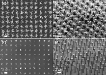
| Xu, et al. demonstrate the low-temperature (<100 °C) growth of size-controlled, patterned ZnO nanowire arrays onto multiple types of substrates. |
Reviewed by Prof. Aaron E. Saunders, Department of Chemical & Biological Engineering, University of Colorado at Boulder
- Xu, et al. Patterned Growth of Vertically Aligned ZnO Nanowire Arrays on Inorganic Substrates at Low Temperature without Catalyst. Journal of the American Chemical Society, 2008, 130(45), 14958-14959. DOI: 10.1021/ja806952j
One significant challenge in nanomanufacturing is the development of simple techniques to deposit or grow nanomaterials uniformly across large regions, while simultaneously controlling the spacing and arrangement of the individual particles or structures. While self-assembly techniques can be used to deposit colloidal nanomaterials from solution to form ordered superlattice films, it is challenging to use such methods to create non-periodic arrays or films that are not close-packed.
Recent efforts to grow nanomaterials directly onto substrates or devices has met with some success, though challenges still remain in devising synthetic routes that are compatible with the standard lithographic approaches used to form integrated circuits. A recent article from Z. L. Wang’s group at Georgia Tech (Xu, et al., JACS, 2008, 130(45), 14958-14959) demonstrates a new technique to grow arrays of aligned ZnO nanowires onto a variety of inorganic substrates, without the use of metal catalysts or extreme synthesis conditions that could disrupt underlying device structures.

In this method, a substrate is first coated with a 50 nm thin film of polycrystalline ZnO, to serve as seeds for nanowire growth. To direct the size and arrangement of the nanowires, a PMMA film is deposited onto the substrate and patterned using electron beam lithography. The patterned substrate is then floated in a solution containing the nanowire precursors for up to 24 hours, resulting in the nucleation and growth of uniform ZnO nanowires from the exposed seeds (Figure 1). By varying the temperature, Xu et al. were able to grow single or multiple nanowires from each exposed seed, and could generate defect-free arrays covering areas up to 200 μm x 200 μm.
While the use of this technique for large-scale production will depend on the ability to implement this procedure using standard UV-light lithography or other large-area patterning techniques, the ability to arbitrarily pattern structures under relatively benign conditions is a significant step toward incorporating ZnO nanomaterials into different microelectronic devices.
Image reproduced with permission from Xu, et al. Patterned Growth of Vertically Aligned ZnO Nanowire Arrays on Inorganic Substrates at Low Temperature without Catalyst. Journal of the American Chemical Society, 2008, 130(45), 14958-14959. Copyright 2008 American Chemical Society.
This work is licensed under a Creative Commons Attribution-NonCommercial-NoDerivs 3.0 Unported.
