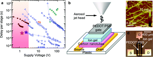
| Integration of electronic circuits on flexible substrates is important for innovative displays, sensors, and electronic systems. Fabrication approaches commensurate with roll-to-roll and print process platforms will enable low cost, high throughput manufacturing to meet the targets associated with these emerging applications. Yet thin film transistor technologies typically suffer from low carrier mobility and high switching voltages that limit the upper frequency at which the transistors can operate. Recently, Ha et. al. reported on digital circuits fabricated from CNT thin films printed on plastic and silicon dioxide substrates. In their approach, the combination of the high purity CNT films along with the high capacitance ion gel gate dielectric provides the low voltage, high speed circuitry performance in comparison to previous thin film transistor material and device designs. |
Reviewed by Jeff Morse, PhD., National Nanomanuafcturing Network
Integration of electronic devices and circuits on flexible substrates is important for applications such as flexible displays, large area sensors, and smart tape electronic systems. Establishing fabrication approaches commensurate with roll-to-roll and print process platforms will enable low cost, high throughput manufacturing to meet the targets associated with these emerging applications. Yet thin film transistor technologies like organic and nanoparticle-based semiconductors typically suffer from low carrier mobility and high switching voltages that limit the upper frequency at which the transistors can operate. Thus a key remaining challenge in printable circuits resides in achieving high performance materials, devices, and circuits.
Strategies to establish high performance circuits integrated on flexible substrates include silicon chips bonded to flexible substrates via transfer printing or pick-and-place methods, which offer the superior performance and maturity of silicon integrated circuits, yet suffer from limited throughput and higher costs in comparison to solution-based approaches compatible with printing processes. Previously, both printed and non-printed versions of ring oscillator circuits have been fabricated with the latter demonstrating switching delays of 1-10 µs, but requiring very high gate voltages. On the other hand devices having low switching voltages (4-10 V) typically exhibit switching time >1 ms.

In order to push the envelope of shorter delay times and lower switching voltages for printed electronics, carbon nanotube (CNT) transistors have gained a great deal of attention, mainly as a result of the large intrinsic mobility (~100,000 cm2/V-s) of single semiconducting CNTs. CNT thin films, deposited either from solution or dry transfer processes, have been developed as an approach toward scaled-up printed electronics. Recently, Ha et. al. reported on digital circuits fabricated from CNT thin films printed on plastic and silicon dioxide substrates. The authors started with water-based, sorted CNT inks prepared by density gradient ultracentrifugation using arc-discharge grown CNTs (Carbon Solutions, Inc. ). The purity level of the CNTs was determined to be 98% semiconducting using optical absorbance spectroscopy, with the remainder being metallic in nature. The sorted CNT inks were dialyzed into a 0.2% w/v sodium cholate aqueous solution. Both polyimide and oxidized silicon substrates were prepared with pre-patterned CrAu electrodes to define the transistor channel and interconnects. Nominal channel dimensions were 500 µm wide by 50 µm in length. Printing of the CNT ink was accomplished using a commercial aerosol jet printing system, and the CNT coverage on the surface was controlled by the concentration of the ink and the print speed. The authors determined that a surface coverage of 30% CNTs provided optimal ON/OFF current ratios for the thin film transistors. The deposited CNTs were rinsed and baked in order to remove any residual solvents. The CNT thin film was followed by deposition of a high capacitance ion gel dielectric ink printed over the channel, followed by a gate electrode formed from a conducting polymer poly(3,4-ethylenedioxythiophene):poly(styrenesulfonate) (PEDOT:PSS) printed over the ion gel dielectric.
Electrical testing and characterization of digital inverter and ring oscillator circuits exhibited an ON/Off current ratio of >104 for VD =-0.1 V, and effective carrier mobilities were estimated to be 30 and 20 cm2/V-s for electrons and holes respectively, much higher than previously reported. Switching delays as short as 50 µs were measured for ring oscillator circuits owing to the gate sheet capacitance estimated to be ~10 µF/cm2. Additionally, the CNT thin film transistors exhibited ambipolar behavior—depending on the bias conditions, the transistors could exhibit either p-type or n-type device behavior—therefore a common transistor design could provide complimentary logic circuit designs.
In this approach, the combination of the high purity CNT films along with the high capacitance ion gel gate dielectric provides the low voltage, high speed circuitry performance in comparison to previous thin film transistor material and device designs. Furthermore, the process is compatible with high-rate, low-cost roll-to-roll printing processes. Additional research will investigate methods to reduce channel dimensions and further control the impact of quantum capacitance effects that potentially can dominate the gate capacitance for certain device designs.
Image reproduced with permission from Ha M, et al. 2010. ACS Nano 4(8): 4388–4395. DOI: 10.1021/nn100966s. Copyright 2010 American Chemical Society.
This work is licensed under a Creative Commons Attribution-NonCommercial 3.0 Unported.
