

Traditional roadmapping struggles to deal with discontinuous change. It's not easy to predict when a new technology will become cost competitive, how it can scale to meet market needs, how the existing technologies can be tweaked to meet the performance challenge of new materials - or even which technologies will win and who will develop them! It becomes a situation where multiple scenarios are possible and the experts in the room have to make a best judgement based on the available information.
Currently, nanostructures appear to be limited to semiconductors and hydrophobic/oleophobic surfaces. Nanomaterials or near-nano materials are increasingly found in batteries, supercapacitors, silver for die attach and solar applications, phosphors and a range of polymer fillers as well as in CMP slurries.
The proposed changes by EPA to TSCA will affect reporting and other requirements for nanomaterials (www.epa.gov/oppt/nano/ and available as a Federal Register extract (Vol.80, No.65, April 26, 2015), searchable as EPA-HQ-OPPT-2010-0572-0001) have raised concerns as in some interpretations they appear to cover in-process slurried and suspended materials and other forms which would cover not only previously unregulated parts of the electronics industry but also most of the advanced ceramics industry.
Who will develop the nanomaterial and nanostructures? The financial institutions and angel investors are not supporting the industry well. I personally am working with two electronics startups struggling for survival as most of the angel money goes to handheld apps, VCs are missing in action, and IPOs seem to be limited to pharmaceuticals. Those that are successful will partner with established companies who can supply the "patient money" needed for commercialization and scaling. We do need a lot more corporations to embrace open innovation - rather than "not invented here!" for this to be successful.
The electronics industry needs nanomaterials and nanostructures if it is to meet customer expectations - higher performance, better battery life and more affordable. We need to continue to work with startups and established industry to commercialize the excellent work stimulated by the NNI and now coming out of Universities to make this happen.
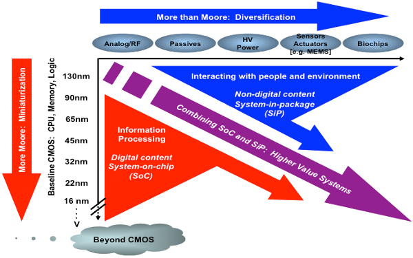
Image credit: Permission to reprint image requested from ITRS.
More than Moore White Paper by the IRC