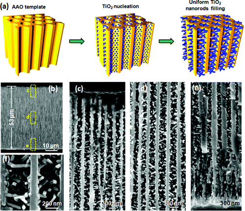
Nanotechnology-enabled fabrication of solar cells with conventional nanoparticle-based thin-films has a drawback in that the diffusion length of the charge carriers is too short to get charge separation, although the nanoparticles themselves provide copious surface areas; whereas photovoltaic devices fabricated by aligned or partially aligned nanowire array configurations have exhibited enhanced performance owing to improved carrier collection, reduced optical reflection, and efficient absorption.
While the nanowire-based approach indeed increases the diffusion length of carriers it also reduces the available surface area. However, being able to fully capture the promising surface and transport properties of nanoscale materials in practical devices or systems relies on the capability of effectively translating the extraordinary characteristics of nanoparticles or nanowires into larger-scale, three-dimensional (3D) structures.
Researchers at the University of Wisconsin-Madison have come up with a promising approach to address this problem. They have successfully grown uniformly distributed and high density nanorods into high-aspect ratio nanochannels. Fabricating such 3D nanowire networks is very challenging by all current strategies but could be dramatically beneficial to the applications of solar cells, sensors, catalysts, and energy storage systems.
As they report in the January 24, 2011, online edition of NANO Letters ("Growth of Titanium Dioxide Nanorods in 3D-Confined Spaces") a team from Xudong Wang's Nanoscience and Nanotechnology group have used a pulsed chemical vapor deposition (CVD) process to grow single-crystalline titanium dioxide nanorods uniformly covering the entire inner surface of highly confined nanochannels.
"The motivation for our work was that we wanted to design an architecture with both plentiful surface area and long enough diffusion length of carriers in one integrated structure," Jian Shi, first author of the paper, tells Nanowerk. "Our technique provides a possible structure that not only inherits the ample surface areas which can be achieved by conformal nanorods coating but also the long diffusion path of carriers which could be achieved by a conductive nanochannel."

Shi explains that, among all bottom-up nanostructure synthesis techniques, atomic layer deposition (ALD) is one excellent approach that produces conformal coating in high aspect ratio channels owing to its self-limiting surface reaction.
"ALD has been widely applied to grow conformal thin film coating with precisely controlled thickness down to the subnanometer level" he says. "A recent discovery has also shown that introducing metal catalysts to the ALD process could lead to the transition from conformal coating to vapor-liquid-solid growth of nanowire morphology. What we are doing in our approach is to mimic the ALD process using separated exposures of gaseous titanium tetrachloride and water precursors at high temperature and extended pulsing and purging times."
This approach, using a homemade ALD system, allowed the team to uniformly grow titanium dioxide nanorod arrays along the entire inner surface of highly confined nanochannels.
"To our best knowledge, this is the first strategy for successfully growing a 3D titanium dioxide nanowire network architecture in highly confined spaces, which might also be applied to a variety of other functional materials" Shi points out. "It could lead to the realization of nanowire-based 3D nanoarchitectures from various functional materials for the applications of sensors, solar cells, catalysts, energy storage systems, and so forth."
These new structures have the potential to significantly improve the performance or efficiency of many electrical and electrochemical devices such as sensors, detoxification filters, hydrogen storage systems, lithium-ion batteries, fuel cells, photovoltaic devices, photocatalysis, or supercapacitors.
The surface area of the team's 3D nanowire architecture is nearly an order of magnitude higher than nanowire arrays and comparable to that of highly-packed nanoparticle films. What makes this 3D structure so promising is that it could also offer charge transport properties as good as that of nanowire-arrays based solar cells.
"Our 3D structure not only inherits the long diffusion path of charge carriers but also has the ample surface area of packed nanoparticle films, which is dramatically important but has never been achieved in previous studies," says Shi. "In addition, crystal quality and size uniformity of the as-grown nanostructures by our method are superior to those achieved by hydrothermal process and conventional chemical vapor deposition techniques."
The team believes that the anisotropic growth of titanium dioxide crystal is the result of the combined effects of the surface-related precursor molecule absorption and reaction.
"We also found the (001) surface of titanium dioxide crystal to be essential for the formation of nanorod morphology" says Shi. "However, further in-depth understanding of the nucleation step is greatly desired for fully revealing the nanorod formation process and allowing us to realize a nanowire-based 3D nanoarchitecture from a variety of functional materials."
Source: Nanowerk
Image reproduced with permission from Shi J, et. al. Growth of Titanium Dioxide Nanorods in 3-D Confined Spaces. Nano Lett., Article ASAP 24 January 2011. doi: 10.1021/nl103702j.
