Skip to content Skip to navigation

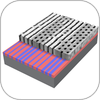
lithography

reproducible creation of a pattern [SOURCE: ISO/TS 80004-8 v1, 3.6]

EV Group
EV Group
DI Erich Thallner Strasse 1 4782 St.Florian am Inn AUSTRIA

Our vision of "being the first in exploring new techniques and serving next generation applications of micro and nano fabrication technologies" enables our customers to successfully commercialize their new product-ideas. This ensures continuous effective development and economic stability.

The basis for our success is our products: lithography, bonding and imprint systems. We hold the dominant share of the market for all types of wafer bonding equipment and are the market and technology leader in lithography and nanoimprinting.


UD Nanofabrication Facility
221 Academy Street Newark, DE 19716 USA

The UD Nanofabrication Facility (UDNF) will enable researchers in academia, industry and government to create devices smaller than a human hair, supporting scientific advances in fields ranging from medical diagnostics to environmental sensing to solar energy harvesting.

Capabilities
The UD Nanofabrication Facility (UDNF), part of the research wing of UD’s Patrick T. Harker Interdisciplinary Science and Engineering Laboratory, has world-class capabilities in the areas of deposition, etching, lithography, material modification and characterization.

Gigaphoton Inc.
Gigaphoton Inc.
400 Yokokurashinden Oyama-shi, Tochigi-ken 323-8558 Japan

Gigaphoton Inc. was founded in 2000 as a leading-edge technology company to support the semiconductor industry in the 21st century. Since then, we at Gigaphoton have been developing and marketing user-friendly, highly innovative laser light sources and delivering them to major lithography tool suppliers in the global semiconductor industry. In addition, we have been aggressively working on the development and mass-production of Extreme Ultra Violet (EUV) light sources as the next-generation lithography light sources.

Heidelberg Instruments Inc.
2539 W 237th St Suite A Torrance, CA 90505 United States

With an installation base of over 850 systems worldwide, Heidelberg Instruments is a world leader in the production of high-precision photolithography systems and maskless aligners.  Due to their flexibility, these systems are used in research, development and industrial applications for direct writing and photomask production by some of the most prestigious universities and industry leaders. Applications include MEMS, BioMEMS, nanotechnology, ASICS, TFT, plasma displays, micro optics and others.