
Electronics and Semiconductor Industries
Quantum Nanostructures and Nanofabrication Group

Department of Electrical Engineering and Computer Science
77 Massachusetts Ave. M/S 36-219
Cambridge, MA 02139
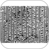
The frontier of electronic and photonic devices lies in nanoscience and nanotechnology research. At the nanoscale, materials and structures can be engineered to exhibit interesting new properties, some based on quantum mechanical effects. Our research focuses on pushing nanofabrication technology to the few-nanometer length-scale by using charged-particle beams combined with self-assembly. We use the technologies we develop to push the envelope of what is possible with photonic and electrical devices, focusing in particular on the nanowire-based superconductive photodetectors.


Carnegie Mellon Nanofab

ECE Department
Pittsburgh, PA
15213
USA
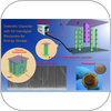
A premier research laboratory in the College of Engineering, the Carnegie Mellon Nanofabrication Facility is one of the most well equipped university based facilities for thin film and nano/micro device development in the United States. The Nanofab includes a cleanroom with 2,600 square feet of class 100 space and 1,200 square feet of class 10 space, as well as three thin film labs.
Nano Dimension

Science Park
3 Golda Meir St.
Ness-Ziona, 74036
Israel
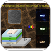
We all wish that developing multi-layer professional PCBs was faster and more flexible. That's why we're making a 3D PCB printer and a suite of nano-technology inks specifically for PCB professionals.
The Nano Dimension PCB printer is a highly accurate and versatile inkjet deposition system for printing multi-layer circuit boards. The innovative hardware, dedicated nano-inks and novel software bring new possibilities to a wide range of R&D, prototyping and custom manufacturing projects. Our highly conductive silver nano-inks are also available separately.