|
The NNN Newsletter
Nanomanufacturing Information Survey
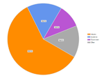 During April and May, the NNN conducted a "Nanomanufacturing Information Survey" among nanotechnology professionals in an effort to understand how people inform themselves about advances in nanomanufacturing and to determine what kinds of information content and formats are most valued. In doing so, the survey provides a snapshot of the current landscape of nanomanufacturing community. During April and May, the NNN conducted a "Nanomanufacturing Information Survey" among nanotechnology professionals in an effort to understand how people inform themselves about advances in nanomanufacturing and to determine what kinds of information content and formats are most valued. In doing so, the survey provides a snapshot of the current landscape of nanomanufacturing community.
Findings from this survey indicate that nanomanufacturing professionals, largely from industry, seek practical, reliable, and technical information on the implementation or integration of nanomanufacturing processes. Ongoing research into the fundamental science of nanomaterials properties and behaviors will contribute to sought after studies on reproducibility and scale-up of advanced processes. Beyond technical implementation, commercialization and cost analyses were identified as being critical pieces of information that are currently difficult to find or to filter out from available information.
Overall, the range of application areas and activities reported in this survey underscores the notion that nanomanufacturing is truly a bridge between discovery and implementation, a crossroads of research and development that reaches across all areas of application and encompasses supplementary functions such as regulation and informatics. In addition, it provides a snapshot of the current range of application areas active in nanomanufacturing, while also indicating to us that nanomanufacturing is still a nascent area of expertise, one that will develop as nanotechnologies mature and make their way to the marketplace with increasing frequency.
More...
Regards,
Jeff Morse, Managing Director,
National Nanomanufacturing Network
Learn More about the 
|
NNN Test Bed Reviews
May 2010
NSF Center for High-rate Nanomanufacturing
Northeastern University, University of Massachusetts Lowell
 Multi-scale Directed Assembly of Polymer Blends Using Chemically Functionalized Nanotemplates Multi-scale Directed Assembly of Polymer Blends Using Chemically Functionalized Nanotemplates
Nanoscale patterned polymeric structures with multiple surface functionalities can be used for the fabrication of microphotonic arrays, biosensors, and semiconductor integrated circuits. The directed assembly of polymer blends into nanoscale structures offers an advantage in that a wide array of polymers and molecular weights are readily available for use. In contrast to block copolymers, blends have greater flexibility in forming non-uniform structures and are not constrained in terms of domain size by the block length. Additionally, the use of chemically functionalized nanotemplates can be exploited to direct the nanoscale assembly of polymer blends into non-uniform patterns in relatively short timescales. The use of a short solvent annealing step allows the preparation of non-uniform geometries and multiple length scales in a single template. More....
|
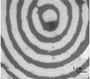
Large Area Synthesis of Graphene Sheets by Metal-Catalyzed Crystallization
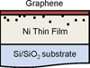 Methods of graphene production have emerged from the initial methods of generating small amounts for research studies—typically by mechanically exfoliating monolayers from bulk graphite—to alternative approaches conducive with large area processing. One approach, using chemical vapor deposition (CVD), takes advantage of existing process tools, yet suffers from difficulty in controlling the number of graphene layers over large areas due to the sensitivity of various process parameters. Recently, Zheng and colleagues describe a method to synthesize large-area, transferrable graphene films by metal-catalyzed crystallization of amorphous carbon (a-C) through thermal annealing. More.... Methods of graphene production have emerged from the initial methods of generating small amounts for research studies—typically by mechanically exfoliating monolayers from bulk graphite—to alternative approaches conducive with large area processing. One approach, using chemical vapor deposition (CVD), takes advantage of existing process tools, yet suffers from difficulty in controlling the number of graphene layers over large areas due to the sensitivity of various process parameters. Recently, Zheng and colleagues describe a method to synthesize large-area, transferrable graphene films by metal-catalyzed crystallization of amorphous carbon (a-C) through thermal annealing. More....
NIST 2010 TIP Competition
 Through July 15th, NIST is accepting proposals for the 2010 Technology Innovation Program. The new TIP competition offers cost-shared funding for innovative research on "Manufacturing and Biomanufacturing: Materials Advances and Critical Processes." The TIP program is designed to address societal challenges by supporting technology innovation in areas of critical national need. Individual companies can receive up to $3M over 3 years, which can support up to 50% of the direct costs of an R&D project. Joint ventures involving two or more companies, universities, or research laboratories are eligible for even larger awards, up to a maximum of $9M over 5 years (again with a minimum 50% of cost sharing). Last year, nanotechnology companies responded enthusiastically to the TIP program call for advanced manufacturing concepts. They were rewarded with 6 funded projects in the application area Process Scale Up, Integration and Design - Nanomaterials. More.... Through July 15th, NIST is accepting proposals for the 2010 Technology Innovation Program. The new TIP competition offers cost-shared funding for innovative research on "Manufacturing and Biomanufacturing: Materials Advances and Critical Processes." The TIP program is designed to address societal challenges by supporting technology innovation in areas of critical national need. Individual companies can receive up to $3M over 3 years, which can support up to 50% of the direct costs of an R&D project. Joint ventures involving two or more companies, universities, or research laboratories are eligible for even larger awards, up to a maximum of $9M over 5 years (again with a minimum 50% of cost sharing). Last year, nanotechnology companies responded enthusiastically to the TIP program call for advanced manufacturing concepts. They were rewarded with 6 funded projects in the application area Process Scale Up, Integration and Design - Nanomaterials. More....
Read more on 
|
Upcoming Events
June 2 - 4, 2010
Nanotoxicology 2010
June 8 - 10, 2010
Nanomaterials 2010
June 15 - 17, 2010
International Conference on Green Remediation
June 21 - 24, 2010
NSTI Nanotech Conference & Expo 2010
June 22 - 24, 2010
New England Nanomanufacturing Summit 2010
View Full Calendar
Advertisement

Upcoming Calls
ASAP!
New England Nanomanufacturing Summit 2010
Deadline for abstracts
June 22, 2010
MRS Fall Meeting
Deadline for abstracts
June 28, 2010
SPIE Nanoscience + Engineering
Deadline for manuscripts
July 30, 2010
3rd Annual Nanotechnology Symposium
Deadline for abstracts
August 30, 2010
BIT's 1st Annual World Congress of Nanomedicine
Deadline for poster abstracts
Recently Published
From Our Affiliates
Placement of alkanethiol-capped Au nanoparticles using organic solvents
Journal of Colloid and Interface Science 346(1):17-22
Effect of Different Deposition Mediums on the Adhesion and Removal of Particles
Journal of the Electrochemical Society 157(6):H662-H665
GaAs Photovoltaics and Optoelectronics Using Releasable Multilayer Epitaxial Assemblies
Nature 465(7296): 329-U80
Free Folding of Suspended Graphene Sheets by Random Mechanical Stimulation
Physical Review Letters 104(16): 166805
Affiliated Centers


|
 Volume
3 Issue 5 - May 2010
Volume
3 Issue 5 - May 2010