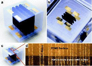
| Engineering of carbon nanotubes (CNT) into controlled morphologies and architectures has progressed to the point where electrodes fabricated from CNT networks have become viable candidates for applications such as flexible electronics, solar photovoltaics, and optoelectronics. Recently, Li et. al. reported on their investigation of forming organized 2D and 3D hybrid single-walled carbon nanotube (SWCNT)-polymer architectures. This paper reports a scalable approach to forming precisely controlled architectures of 3D SWCNT networks for integration of electrical connections. Nominally the approach would be adaptable to a wide range of metal and polymer substrates and could be further scaled down to smaller line width features as well as larger areas. |
Reviewed by Jeff Morse, PhD, National Nanomanufacturing Network
- Li B, Hahm MG, Kim YL, Jung HY, Kar S, Jung JY. 2011. Highly organized two- and three-dimensional single-walled carbon nanotube–polymer hybrid architectures. ACS Nano. 5(6), 4826-4834. doi:10.1021/nn2008782.
Techniques to extend the controlled manipulation of CNTs to achieve multidimensional architectures include directional growth, fluidic assembly, and pattern transfer. Using such approaches, architectures of aligned single and multi-walled CNTs have been demonstrated both in horizontal or vertical orientations. As an example, fluidic assembly methods can be used to selectively assemble densely packed films of CNTs into pre-patterned photoresist trenches by making the resist hydrophobic to the CNT suspension and the trench surface hydrophilic to the suspension. CNT patterns such as this become candidates for electrical leads and connectors for integrated circuits or other multifunctional systems such as microfluidics. As advance circuits and systems are becoming inherently three-dimensional, the next challenge is to form organized architectures of multidimensional CNT networks with the ability to embed the CNTs in a hybrid configuration such as a polymer matrix.

Vertically aligned SWCNTs were grown by ethanol chemical vapor deposition (CVD) using patterned cobalt catalyst on SiO2 coated silicon substrates to precisely control the location and dimensions of vertical CNT forests. To transfer the vertical SWCNT patterns, the SWCNT/ SiO2/Silicon substrate was turned upside down and brought into contact with a thin layer of uncured PDMS spin-coated on another SiO2/silicon substrate. After curing of the PDMS, the SiO2 was selectively etched in HF acid resulting a free-standing vertically aligned SWCNT embedded in the surface of the PDMS film. By controlling the wetting and thickness of the PDMS layer, the extent to which the SWCNTs are embedded can be further controlled. In addition, the authors combined vertically and horizontally aligned SWCNT structures integrated into a 3D electrically conducting network within a polymer matrix. The resistance of the 3D SWCNT architecture was dominated by that of the horizontal SWCNT films, and surprisingly the contact resistance between the vertically and horizontally aligned SWCNTs was only a small percentage of total resistance. The authors were able to show that the SWCNTs could be integrated into a microfluidic gas sensor architecture demonstrating the performance of this concept for this particular application.
Thus a scalable approach to forming precisely controlled architectures of 3D SWCNT networks for integration of electrical connections has been reported. Nominally the approach would be adaptable to a wide range of metal and polymer substrates and could be further scaled down to smaller line width features as well as larger areas.
Figure reprinted with permsision from Li B, Hahm MG, Kim YL, Jung HY, Kar S, Jung JY. 2011. Highly organized two- and three-dimensional single-walled carbon nanotube–polymer hybrid architectures. ACS Nano. 5(6), 4826-4834. doi:10.1021/nn2008782. Copyright 2011 American Chemical Society.
