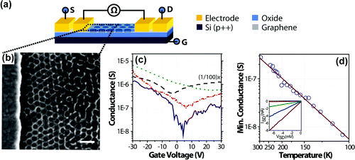
| Kim and colleagues report on a method, using block copolymer (BCP) lithography, for achieving both the critical dimensions and scalability necessary for developing a semiconductor integration strategy for graphene-based devices. The relative ease by which BCP lithography can be implemented and scaled to large areas makes this a practical approach to large-area, commercializable applications for graphene-based electronics. |
Reviewed by Jeff Morse, Ph.D, National Nanomanfuacturing Network
Graphene has received significant scientific attention in recent years due to its unique electronic, thermal, and mechanical properties, notably its potentially large electron mobility (>200,000 cm^2/V-sec). Areas of technological interest for graphene include future high performance electronics, sensors, transparent conductors, and flexible electronics. However, despite graphene’s potentially superior electronic transport properties, the material suffers from the lack of a technologically significant electronic bandgap, thereby limiting the ability to modulate the conductance of graphene-based devices by field or doping effects.
Current modulation is of critical importance for semiconductor device and circuit applications. To implement it, electronic bandgaps have been formed in graphene by way of quantum confinement of the material structure. Examples of this have been demonstrated via graphene nanoribbons and electron beam lithographic patterning, in which both confined individual structures and periodic structures have been investigated. As such, a bandgap dependence for the nanostructured graphene has been observed for critical feature sizes on the order of <20 nm in width.
While advanced electron beam lithography can pattern features having 10 nm critical dimensions, it remains a serial process, consequently limiting throughput and increasing cost for scaled processing. Other methods of synthesizing graphene nanostructures have limited scalability and lack a clear path to integration. Recently, Kim et. al. investigated these challenges using block copolymer (BCP) lithography to provide a facile route to achieving both the critical dimensions and scalability necessary to achieve a semiconductor device integration strategy. BCP lithography has achieved feature resolution <10 nm with scalability demonstrated over relatively large areas, therefore enabling a low-cost method to create graphene nanostructures.

The authors used highly oriented pyrolytic graphite and mechanically exfoliated graphene monolayers to develop the process for BCP patterning. Utilizing the cylinder forming poly(styrene-block-methyl methacrylate) BCP materials system, the authors first coated the graphene films with two intermediate layers to improve adhesion and uniformity. These layers included 10 nm of silicon dioxide to promote wetting, and a random copolymer blend of methyl methacrylate, styrene, and glycidyl methacrylate (MMA, S, GMA) to act as a neutral layer promoting the BCP segregation energetics. The BCP patterning was followed by selective reactive ion etching to transfer the nanoscale patterns into the layers below, ultimately creating a graphene film having nanoscale ordered perforations with nominal constriction features on the order of 18 nm.
The authors fabricated field effect transistor (FET) devices by placing the nanopatterned graphene monolayer on silicon dioxide coated p-type silicon substrate. Using the silicon substrate as the gate electrode, source-drain electrodes were formed on the graphene by conventional lithography and patterning of CrAuTi films. Electrical characterization of the graphene FET exhibited On/Off ratios exceeding 40 and 200 at room temperature and 105 degrees K respectively. Room temperature electron mobility on the order of 2000 cm^2/V-sec was estimated from conductance measurements, and a hole mobility of `1 cm^2/V-sec was estimated, making this material competitive with other transistor devices for flexible substrates.
The relative ease by which BCP lithography can be implemented and scaled to large areas makes this an effective method for controlling the electronic properties of graphene. This versatile and facile approach will potentially enable practical, large-area, commercializable applications for graphene-based electronics.
Image reproduced with permission from Kim M, et al. 2010. Fabrication and Characterization of Large-Area, Semiconducting, Nanoperforated Graphene Materials. Nano Letters 10(4):1125–1131. DOI: 10.1021/nl9032318. Copyright 2010 America Chemical Society.
This work is licensed under a Creative Commons Attribution-NonCommercial 3.0 Unported.
