
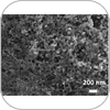
Presented here is a method for assembling homogenous films of controllable thickness comprised of hybrid nanostructures on a roll-to-roll platform directly from solution. Using surfactant-free mixtures of nanoparticles, nanotubes, nanosheets, and any combination thereof, film fabrication may be achieved that maintains the chemical and physical properties inherit to the constituent material that is not limited by the presence of surfactants or impurities. Using this technique, researchers may demonstrate the viability of scalable production of a synthesized material.
Process Database
The InterNano Process Database is a knowledge base of techniques for processing nanoscale materials, devices, and structures that includes step-by-step descriptions, images, notes on methodology and environmental variables, and associated references and patent information.
The purpose of the Process Database is to facilitate the sharing of appropriate process knowledge across laboratories.The processes included here have been previously published or patented.
If you have a published and/or patented process that you would like to include in the InterNano Process Database, you can either contact us and we will add the process for you, or you can register on InterNano and add the process yourself.
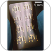
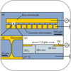
A process for making flexible circuits based on semiconducting carbon nanotube networks and high capacitance ion gel dielectrics through jet printing of liquid inks.
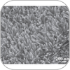
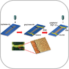
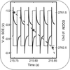
A method for the controlled direct growth of highly crystalline ZnO nanorods on a paper substrate is described. Despite the complexity and surface roughness which paper naturally presents, adequate surface modification enhances ZnO nanorod alignment and uniformity in growth. Large scale synthesis is also demonstrated. Hybrid PN junction diodes, also on paper substrates, show application toward flexible electronics.
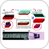
The approach of transferring CNT thin films from one surface to another via a soft lithography technique suffers from limited ability to achieve good adhesion of the CNT films to the transferred substrate and imprecise alignment of the CNT patterns. A transfer technique that can be scaled to large area with high throughput processing at low temperature is being reported in this paper, demonstrating a scalable means to create aligned CNT thin film patterns on both rigid and flexible substrates.
The serial mechanical exfoliation method available can not be used for the assembly of graphene in the large scale. In this process, deposition of ultrathin few-layer (three to ten) graphene oxide, with parallel and controllable assembly, by dielectrophoresis between prefabricated electrodes has been demonstrated.
Inkjet printing is a promising technique for printing of electronic materials and devices over large areas on flexible substrates. Inkjet printing is a versatile approach involving a limited number of steps with the ability to deposit controlled amounts of material. The development of inks for inkjet printing can be tailored to optimize the properties of the printed films and structures, and are additionally versatile in that virtually any nanomaterial composition can be incorporated as long as the nanostructure size is sufficiently small that the inkjet nozzle does not become clogged.
Phosphine-stabilized gold nanoparticles have a rich chemistry and are excellent building blocks for functional groups, however they have typically been synthesized through cumbersome and unsafe methods. This process is a safer, more convenient, and more versatile procedure to synthesize small, phosphine-stabilized gold nanoparticles under ambient conditions.
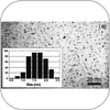
A simple method to control the size of Au nanoparticles via heat treatment. The Au nanoparticles grew to between 3 and 10 nm in size at 150 to 250 degrees C.
Cobalt nanowires with high perpendicular magnetic anisotropy are formed in a diblock copolymer film template using a pulse-reversed voltage with QCM monitoring. This in situ monitoring system along with the pulse-reversed field enables new control over the magnetic crystal growth.

A perpendicular orientation of cylindrical microdomains in diblock copolymer thin films is achieved by control over polymer-surface interactions. The block which forms cylindrical microdomains is removed by UV exposure and a chemical rinse to yield a nanoporous polymer film. The porous film can be used as a template for electrodeposition of metal nanodots or as a mask for reactive ion etching.