Skip to content Skip to navigation

High-yield dielectrophoretic assembly of two-dimensional graphene nanostructures

The serial mechanical exfoliation method available can not be used for the assembly of graphene in the large scale. In this process, deposition of ultrathin few-layer (three to ten) graphene oxide, with parallel and controllable assembly, by dielectrophoresis between prefabricated electrodes has been demonstrated.

Contributors: 

Brian R. Burg, Fabian Lütolf, Julian Schneider, Niklas C. Schirmer, Timo Schwamb, Dimos Poulikakos

Lab: 

Laboratory of Thermodynamics in Emerging Technologies, ETH Zurich, 8092 Zurich, Switzerland

Depositor: 
Amulya Gullapalli
Manufactured Material or Structure: 
Assembly of graphene nano structures
Chip schematic. (a) illustrates the bias electrode used for applying the bias potential from the arbitrary function generator and the counter electrodes, which are capacitively coupled to the conductive substrate except for one, which is directly coupled to the ground. Inset (b) shows in detail the finger electrodes in yellow, over which the two-dimensional graphene nanostructures will bridge. The cross section of the finger electrode gap is depicted in (c). Reprinted from Burg BR, Lutolf F, Schneider J, Schirmer NC, Schwamb T, Poulikakos D. 2009. High-yield dielectrophoretic assembly of two-dimensional graphene nanostructures. Applied Physics Letters. 94(5). Permission pending.
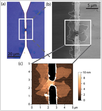
Dielectrophoretic FLGO deposition. (a) Light microscopy image showing the palladium electrodes and revealing the accumulation of FLGO in the regions of highest field gradients. (b) SEM image of the same position with clearly visible contours of the flakes. (c) AFM image of the identical location, showing overlapping layers, twists, and creases of the thin film. Individual GO layers are found near the edges of the electrodes. Reprinted from Burg BR, Lutolf F, Schneider J, Schirmer NC, Schwamb T, Poulikakos D. 2009. High-yield dielectrophoretic assembly of two-dimensional graphene nanostructures. Applied Physics Letters. 94(5). Permission pending.
Step 1:

1 g of natural graphite flake is mixed for 5 days in a 62.1 ml solution of concentrated H2SO4 containing 0.75 g NaNO3 and 4.5 g KMnO4.

Step 2:

Then it is washed in 100 ml 5 wt % H2SO4 and reacted with 3 g of 30 wt % H2O2 in H2O.

Step 3:

Impurities are removed by multiple (15×) centrifugation and ultrasonic precipitate re suspension in aqueous 3 wt % H2SO4 and 0.5 wt % H2O2.

Step 4:

After washing the solution with H2O on a cellulose suction filter 16–40 µm pore size and letting the dispersion rest for 1 day, a last centrifugation cycle (8×) in H2O is performed with the supernatant half of the solution.

Step 5:

After drying the single-layer particles, they are ultrasonically redispersed in water at a concentration of 1 mg/ml.

Step 6:

A droplet (5µl) of the aqueous GO solution is dispensed on the chip, and a sinusoidal potential difference is applied to the bias electrode.

Step 7:

After 60 s the generator is switched off, the droplet is blown off by a stream of nitrogen gas, and the is chip rinsed in de-ionized water.

Step 8:

The sample is characterized by light microscopy, scanning electron microscopy SEM, atomic force microscopy AFM, and electric transport measurements.

Process Notes: 
  1. Thermal annealing of the samples is performed in a rapid thermal anneal oven J.I.P. Elec JetFirst 100 in an inert N2 environment.
  2. Reduction in the FLGO thin lms is confirmed by a sheet conductivity increase and decrease in layer thickness.
Raw Materials: 
  • 1 g of natural graphite flake
  • 62.1 ml solution of concentrated H2SO4 containing 0.75 g NaNO3 and 4.5 g KMnO4
  • 100 ml 5 wt % H2SO4
  • 3 g of 30 wt % H2O2 in H2O
  • exfoliated graphene oxide
Equipment Requirements: 
  • Centrifuge
  • Ultrasonic
  • function generator
  • scanning electron microscopy
  • atomic force microscopy
References: 
Burg BR, Lutolf F, Schneider J, Schirmer NC, Schwamb T, Poulikakos D. 2009. High-yield dielectrophoretic assembly of two-dimensional graphene nanostructures. Applied Physics Letters. 94(5).