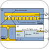
The serial mechanical exfoliation method available can not be used for the assembly of graphene in the large scale. In this process, deposition of ultrathin few-layer (three to ten) graphene oxide, with parallel and controllable assembly, by dielectrophoresis between prefabricated electrodes has been demonstrated.
Deposition of Nanostructured Films or Nanostructures
- Additive processing
- Adsorption
- Atomic layer deposition (ALD)
- Catalytic chemical vapour deposition (CCVD)
- Chemical vapor deposition (CVD)
- Cluster beam coating
- Cold gas dynamic spraying
- Dip Coating
- Electro-spark deposition
- Electro-spray
- Electrodeposition
- Electroless deposition
- Electroplating
- Electrospinning
- Evaporation
- Focused ion-beam (FIB) deposition
- Freeze drying
- Hot wall tubular reaction
- Inductive coupled plasma (ICP)
- industrial polymers
- Ion induced deposition
- layer-by-layer (LbL)
- Modulated elemental reactant method
- Molecular beam epitaxy (MBE)
- Physical vapor deposition (PVD)
- Polyelectrolyte layer-by-layer (LbL)
- Prompt inorganic condensation
- Pulse layer deposition
- Pyrogenesis
- Sol-gel processing
- Solution precursor plasma spray
- Spin coating
- Sputter deposition
- Surface polymerization
- Suspension combustion thermal spray
- Tape casting
- Thermal spray
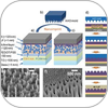
Cobalt nanowires with high perpendicular magnetic anisotropy are formed in a diblock copolymer film template using a pulse-reversed voltage with QCM monitoring. This in situ monitoring system along with the pulse-reversed field enables new control over the magnetic crystal growth.