Skip to content Skip to navigation

Nanocomposites

solids comprising a mixture of two or more phase-separated materials, one or more being nanophase [SOURCE: ISO/TS 80004-4:2011, 3.2.]

Metamaterial Technologies Inc.
1 Research Drive Dartmouth, Nova Scotia B2Y 4M9

Our team specializes in metamaterial research, nanofabrication, and computational electromagnetics; bridging the gap between the theoretical and the possible. With our in-house design, access to world-class nanocomposite research, and nanofabrication expertise, we are able to develop a wide array of metamaterial applications which encompass several industries including aerospace and defence, healthcare, energy, education, and clean-tech.

Our company is headquartered in Halifax, Nova Scotia and has offices in London, England and Pleasanton, California.

High-Performance Materials Institute
Materials Research Building 2005 Levy Ave. Tallahassee, FL 32310

The High-Performance Materials Institute (HPMI) is a multidisciplinary research institute at Florida State University. HPMI strives to recruit, develop and retain top quality faculty and staff who will develop HPMI into a center of excellence for research and education in the field of advanced materials. Leading edge, revolutionary technology comes as the result of creativity, vision, talent, dedication and teamwork.

N12 Technologies, Inc.
85 Bolton Street Cambridge, MA 02140

N12 is a Cambridge, Massachusetts-based startup that’s commercializing revolutionary nanotechnology to enhance composite materials. Based on MIT-developed and exclusively licensed vertically aligned carbon nanotube (VACNT) technology, N12 has created the world’s first commercial-scale continuous manufacturing capability for its Nanostitch™ product. Nanostitch™ improves shear properties of carbon-fiber and other composite materials by 10-40% and lengthens fatigue life 100 fold.

Fullerex Ltd
Fullerex Ltd
2 Palace Road 2nd Floor East Molesey, Surrey KT8 9D UK

At Fullerex, we seek to support the advancement of nanotechnology in order to create radical, transformative and sustainable improvement to society. We are dedicated to achieving these aims by accelerating the commercialisation and usage of nanomaterials across industry and beyond.

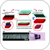
(a) Scheme depicting the process for dry contact transfer of aligned SWNTs as described in the text. (b) SEM image of an upright patterned growth prior to transfer, and (c) picture showing a complete transfer to a 5 mm × 5 mm wide diamond window.
Aligned Carbon Nanotube Patterning Via Dry Contact Transfer Printing

The approach of transferring CNT thin films from one surface to another via a soft lithography technique suffers from limited ability to achieve good adhesion of the CNT films to the transferred substrate and imprecise alignment of the CNT patterns. A transfer technique  that can be scaled to large area with high throughput processing at low temperature is being reported in this paper, demonstrating a scalable means to create aligned CNT thin film patterns on both rigid and flexible substrates.

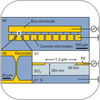
Chip schematic. (a) illustrates the bias electrode used for applying the bias potential from the arbitrary function generator and the counter electrodes, which are capacitively coupled to the conductive substrate except for one, which is directly coupled to the ground. Inset (b) shows in detail the finger electrodes in yellow, over which the two-dimensional graphene nanostructures will bridge. The cross section of the finger electrode gap is depicted in (c). Reprinted from Burg BR, Lutolf F, Schneider J, Schirmer NC, Schwamb T, Poulikakos D. 2009. High-yield dielectrophoretic assembly of two-dimensional graphene nanostructures. Applied Physics Letters. 94(5). Permission pending.
High-yield dielectrophoretic assembly of two-dimensional graphene nanostructures

The serial mechanical exfoliation method available can not be used for the assembly of graphene in the large scale. In this process, deposition of ultrathin few-layer (three to ten) graphene oxide, with parallel and controllable assembly, by dielectrophoresis between prefabricated electrodes has been demonstrated.

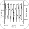
Dotted line: electrode potential, solid line: current, dashed line: EQCM frequency change
Pulse-reversed electrodeposition with QCM monitoring to make magnetic nanowires in a nanotemplate

Cobalt nanowires with high perpendicular magnetic anisotropy are formed in a diblock copolymer film template using a pulse-reversed voltage with QCM monitoring.  This in situ monitoring system along with the pulse-reversed field enables new control over the magnetic crystal growth.

Fabrication of a nanoporous template from a diblock copolymer film - neutral brush

A perpendicular orientation of cylindrical microdomains in diblock copolymer thin films is achieved by control over polymer-surface interactions. The block which forms cylindrical microdomains is removed by UV exposure and a chemical rinse to yield a nanoporous polymer film. The porous film can be used as a template for electrodeposition of metal nanodots or as a mask for reactive ion etching.

Pages