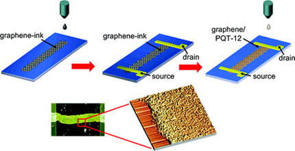
Electronic devices on flexible substrates has been a growing area for research and development due to rapidly expanding applications and markets for touch screens, electronic paper and displays, photovoltaics, lighting, and sensor tags. To achieve the economy of scale for large area substrates requiring active transistor functionality, the primary focus has been to fabricate the electronics directly on the flexible substrate. A typical drawback of this approach is that the fabrication processes must be compatible with the nominally low-temperature plastic materials that are being considered for the substrates. As a result, the semiconductor materials have relatively poor electronic transport properties, which can translate to large switching voltages, as well other performance limitations such as switching current ON/OFF ratio. The most promising materials and processes to date include thin-film metal oxide materials deposited by moderate temperature processes such as chemical vapor deposition (CVD) or atomic layer deposition (ALD), yet there are still concerns associated with substrate compatibility, throughput, and subsequent process integration for final device and circuit designs. In contrast, a range of semiconducting nanomaterials ink formulations have been studied suitable for coating by techniques such as spin-casting, roll-to-roll processing, or inkjet printing. The problems associated with these materials approaches include stability of ink formulations, control over materials dispersion within coatings, and poor electronic transport properties. For the latter, carrier mobility is in .01-0.1 cm2/V-sec, with some examples reported in the 30-50 cm2/V-sec range under controlled process conditions.

Using EG dispersed in N-methylpyrrolidone (NMP) with a composition of 80 wt% EG/20 wt% NMP, inkjet-printed patterns were evaluated for substrates having varying surface energies. The substrates used included pristine silicon dioxide (SiO2), along with plasma treated and surfactant coated SiO2 surfaces, in order to tailor the surface energy, hence the wettability of the surface. Inkjet printed traces on the order of ~100 µm wide were patterned by sequentially depositing drops every 40 µm to create a continuous line. The electrical properties of the deposited coatings were tested. It was found that the surface having the highest contact angle provided the most consistent, homogeneous films as the EG particles were evenly dispersed to the edges. Surfaces that provided enhanced wetting of the ink had increasingly larger spacing between the EG particles closer to the line edge, resulting in larger resistivity, and reduced carrier mobilities. The graphene ink was used to print TFTs with estimated mobilities up to ∼95 cm2/V-sec. The current ON/OFF ratio of the graphene TFT was relatively low (~10) as a result of the graphene film thickness, and ability to fully modulate the current with the gate voltage. While the specific transistor design and performance requires further optimization, these results demonstrate the viability of graphene ink formulations for inkjet printed flexible and transparent electronics. The ink preparation technique can be further generalized for a wide range of layered materials that can also undergo liquid phase exfoliation. These could then be mixed or printed to form hybrid heterostructures with novel properties.
Reviewed by Jeff Morse, PhD, National Nanomanufacturing Network
- Torrisi F, Hasan T, Wu W, Sun Z, Lombardo A, Kulmala TS, Hsieh GW, Jung S, Bonaccorso F, Paul PJ, Chu D, Ferrari AC. 2012. Inkjet-printed graphene electronics. ACS Nano. Article ASAP. http://dx.doi.org/10.1021/nn2044609
Figure reprinted with permission from Torrisi F, Hasan T, Wu W, Sun Z, Lombardo A, Kulmala TS, Hsieh GW, Jung S, Bonaccorso F, Paul PJ, Chu D, Ferrari AC. 2012. Inkjet-printed graphene electronics. ACS Nano. Article ASAP. http://dx.doi.org/10.1021/nn2044609. Copyright 2011 American Chemical Society.
