NSF Center for Hierarchical Manufacturing (CHM), University of Massachusetts Amherst

In this test-bed demonstration, four core technologies are combined to provide a unique manufacturing route for the rapid and cost effective integration of hierarchical metal oxides in which structure is generated and controlled simultaneously at both the nanoscale and the device levels and the need for pattern etching in the oxide is eliminated: ordered block copolymer (BCP) templates, 3-D replication, Nanoimprint Lithography (NIL), and conformal supercritical fluid (SCF) deposition. A full-wafer SCF tool and NIL facility provide tool platforms for subsequent scale-up and application validation.
Impact
This test-bed element enables the fabrication and integration of hierarchical metal oxide films for ultra low k (ULK) dielectric applications and creation of nanofluidic networks.
Challenges, Issues, and Methods
- Minimization of pore size and control of nanostructure by BCP templating;
- Hierarchical template generation by low cost manufacturable patterning;
- Fabrication of nanoporous, metal oxide thin films suitable for use in integrated circuit back end of line (BEOL) applications (including optimization of mechanical properties);
- Demonstration of high throughput patterning strategies for incorporation of ultra low k (ULK) (k<2.5) films in IC applications, exceeding ITRS-defined mechanical and electrical properties;
- Demonstrate the fabrication of microfluidic and nanofluidic channel networks for “lab-on-a-chip” implementations.
Progress
Hierarchical silica films with features spanning two discrete length scales were fabricated using two approaches.
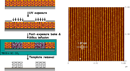
- Demonstrate the supercritical CO2 infusion process to generate domain level, mesoporous silica structures through the 3D replication of amphiphilic block copolymer morphologies from photolithographically patterned device structures (Figure 1).
- Verify the mechanical and electrical properties of ULK films produced by the 3-D replication technique. Mesoporous silica films with enhanced mechanical performance were prepared by incorporating polyoligomeric silsesquioxanes into the organosilicate structures. These films exhibited a hardness of greater than 1.1 GPa at a dielectric constant (k) of 2.3, which is a substantial improvement over leading commercial candidates produced by plasma enhanced chemical vapor deposition (k = 2.4, hardness = 0.7 GPa).
- Combine supercritical CO2 infusion and nanoimprint lithography (NIL) to create complex, embedded device or nanochannel structures through pattern transfer into a polymeric resist material.
- Demonstrate the 3-D replication technique using supercritical CO2 infusion of ordered BCP templates for the production of microfluidic structures with aligned nanochannels of precisely controlled diameter and functionality. These systems are ideal for diagnostics and on-chip separations of biomolecules, including proteins and DNA.
Industry Sectors of Interest
This test bed has achieved the most critical goals set forth at its inception. The films produced are of high quality and meet the integration standards of the semiconductor industry. The materials have been evaluated at several industry labs with results that confirm those reported here. The next steps require integration into functional interconnect structures, along with subsequent reliability and yield testing.

For More Information Contact: Prof. Ken Carter, krcarter@polysci.umass.edu
References
- Romang, A.; Watkins, J. J., Supercritical Fluids for the Fabrication of Semiconductor Devices: Emerging or Missed Opportunities. Chemical Reviews in press 2009.
- Nagarajan, S.; Bosworth, J. K.; Ober, C. K.; Russell, T. P.; Watkins, J. J., Simple fabrication of micropatterned mesoporous silica films using photoacid generators in block copolymers. Chemistry of Materials 2008, 20, (3), 604-606.
- Nagarajan, S.; Russell, T. P.; Watkins, J. J., Dual-Tone Patterned Mesoporous Silicate Films Templated From Chemically Amplified Block Copolymers. Advanced Functional Materials 2009, 19, (17), 2728-2734.
Pai, R. A.; Humayun, R.; Schulberg, M. T.; Sengupta, A.; Sun, J. N.; Watkins, J. J., Mesoporous silicates prepared using preorganized templates in supercritical fluids. Science 2004, 303, (5657), 507-510. - Gates, S. M.; Grill, A.; Dimitrakopoulos, C.; et. al. A porous SiCOH dielectric with k=2.4 for high performance BEOL interconnects. In Advanced Metallization Conference 2006, Russell, S. W.; Mills, M. E.; Osaki, A.; Yoda, T., Eds. 2007; pp 351-357.
- rill, A., Porous pSiCOH Ultralow-k Dielectrics for Chip Interconnects Prepared by PECVD. Annual Review of Materials Research 2009, 39, 49-69.
- Gungor, M. R.; Watkins, J. J.; Maroudas, D., Mechanical behavior of ultralow-dielectric-constant mesoporous amorphous silica. Applied Physics Letters 2008, 92, (25).
- Ell, J.; Crosby, T. A.; Peterson, J. J.; Carter, K. R.; Watkins, J. J., Formation of SiO2 Air-gap Patterns through scCO2 Infusion of NIL Patterned PHEMA. Chemistry of Materials in press 2009.
- Chen, H. T.; Crosby, T. A.; Park, M. H.; Nagarajan, S.; Rotello, V. M.; Watkins, J. J., Accessibility of cylindrical channels within patterned mesoporous silica films using nanoparticle diffusion. Journal of Materials Chemistry 2009, 19, (1), 70-74.
This work is licensed under a Creative Commons Attribution-NonCommercial 3.0 Unported.
